Chemical dispensing system for semiconductor wafer processing

a technology of chemical dispensing system and semiconductor wafer, which is applied in the direction of chemistry apparatus and processes, cleaning processes and apparatuses, coatings, etc., can solve the problems of excessive photoresist collection, and achieve the effect of improving the edge profile of the coating material and increasing the effectiveness of the conventional edge bead removal system

Inactive Publication Date: 2008-12-30
MICRON TECH INC
View PDF53 Cites 6 Cited by
  • Summary
  • Abstract
  • Description
  • Claims
  • Application Information

AI Technical Summary

Benefits of technology

[0005]Accordingly, it is one object of the invention generally to increase the effectiveness of conventional edge bead removal systems. It is another object to control solvent and particle splashing during the process of removing the edge bead from the coating material. It is a further object of the invention to improve the edge profile of the coating material. These and other objects and advantages may be achieved in general by a method for dispensing a chemical, such as an edge bead removal solvent, onto a semiconductor wafer. The method comprises the steps of dispensing the chemical selectively onto the wafer and applying a suction to the area immediately surrounding the location at which the chemical is dispensed onto the wafer. Preferably, the suction is applied substantially simultaneously with the dispensing of the chemical.

Problems solved by technology

In practice, however, some excess photoresist tends to collect at and form a bead along the edge of the wafer.
In either case, the process allows solvent and dissolved photoresist to be splashed about and often leaves a jagged edge profile on the photoresist or other coating material.

Method used


Image

  • Chemical dispensing system for semiconductor wafer processing
  • Chemical dispensing system for semiconductor wafer processing
  • Chemical dispensing system for semiconductor wafer processing

Examples


Embodiment Construction

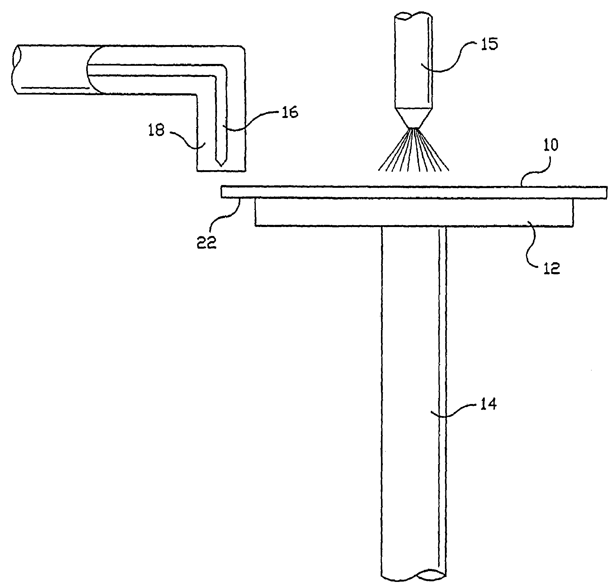
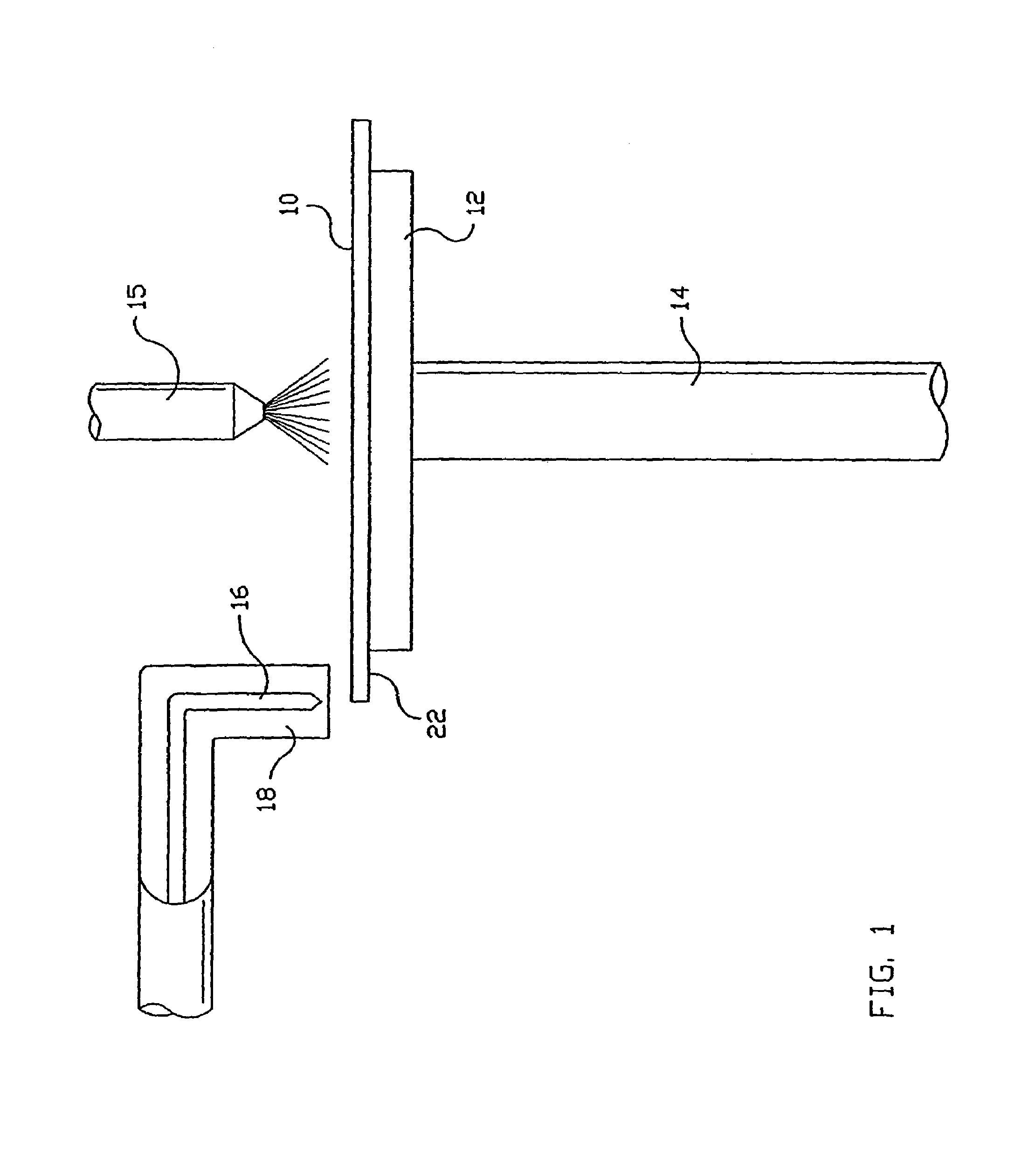
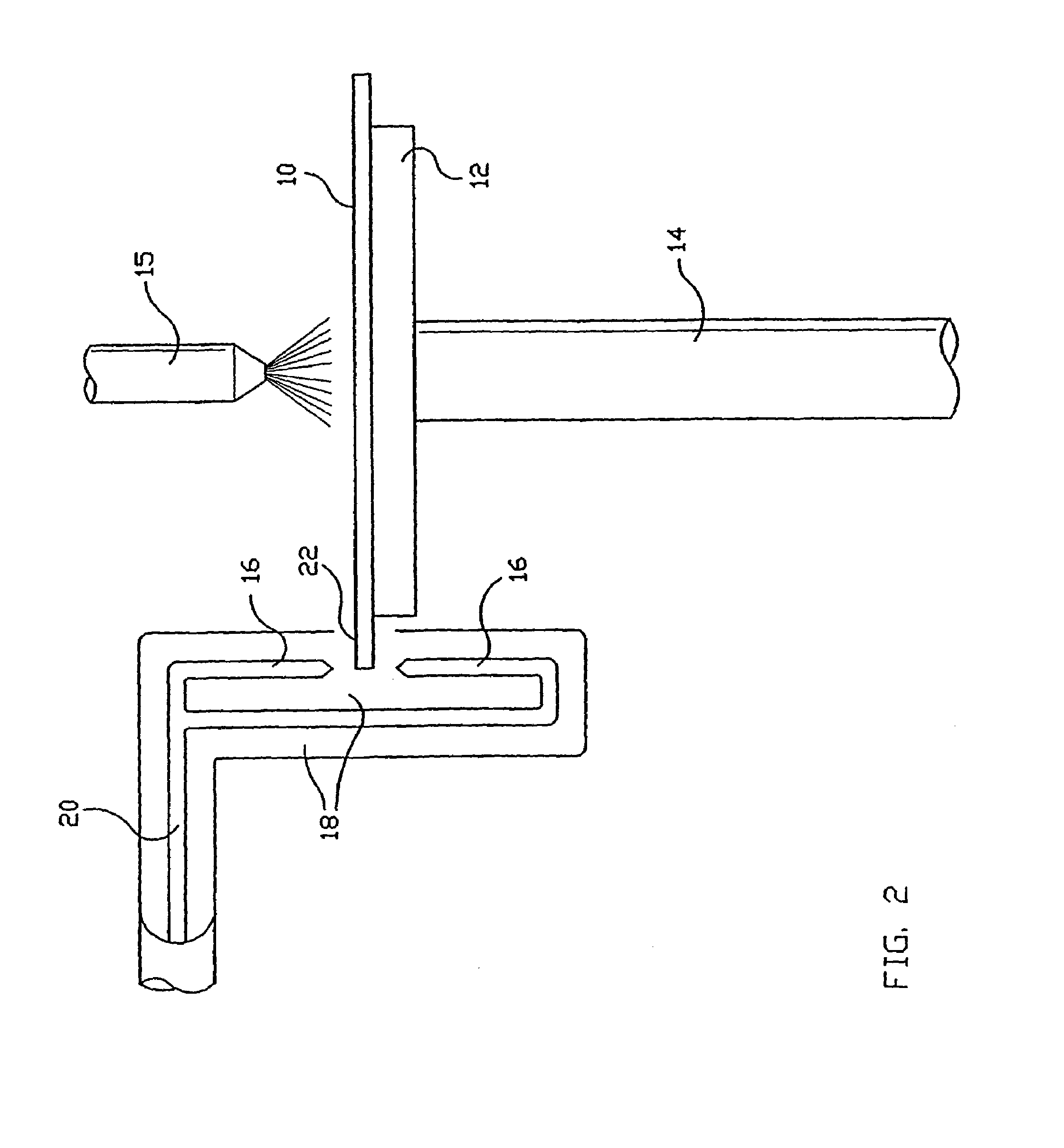
[0009]Referring to FIG. 1, wafer 10 is positioned on spin chuck 12. Spin chuck 12 is mounted on axle 14. Axle 14 is operatively coupled to a drive mechanism, such as an electric motor (not shown). The diameter of spin chuck 12 is less than the diameter of wafer 10 so that wafer 10 extends beyond the edge of spin chuck 12. a first nozzle 15 for dispensing coating material onto wafer 10 is positioned above and, typically, at the center of wafer 10. A second nozzle 16 for dispensing solvent to dissolve the edge bead is disposed above the edge of wafer 10. Solvent dispensing nozzle 16 is surrounded by vacuum port 18. Vacuum port 18 is operatively coupled to a source of negative pressure, such as a vacuum pump (not shown).

[0010]In operation, a suction is applied to the wafer 10 to hold it in place on spin chuck 12. Spin chuck 12 is rotated to spin wafer 10 as a solution of coating material, such as photoresist, is applied through first nozzle 15. Although photoresist is used herein as on...


PUM

PropertyMeasurementUnit
pressureaaaaaaaaaa
diameteraaaaaaaaaa
semiconductoraaaaaaaaaa

Abstract

A method for dispensing a chemical, such as an edge bead removal solvent, onto a semiconductor wafer comprising the steps of dispensing the chemical selectively onto the wafer and applying a suction to the area immediately surrounding the location at which the chemical is dispensed onto the wafer. Preferably, the suction is applied substantially simultaneously with the dispensing of the chemical. One specific version of the invention provides an edge bead removal system wherein suction is applied to the area immediately surrounding the solvent dispensing nozzle to remove dissolved coating material and excess solvent from the wafer. In one aspect of this system, an apparatus for removing the edge bead includes a mechanism for dispensing a solvent selectively onto the edge of the wafer, and a mechanism surrounding the dispensing mechanism for vacuuming excess solvent and dissolved coating material from the edge of the wafer. The edge bead removal apparatus preferably also includes mechanisms for spinning the semiconductor wafer and coating material on the spinning wafer. Another aspect of the system provides a method for removing an edge bead of a coating of material that has been spun onto the surface of a semiconductor wafer. The method includes the steps of dispensing a solvent selectively onto the edge of the wafer to dissolve the coating material at the extreme edge of the wafer, and applying a suction to vacuum excess solvent and dissolved coating material from the wafer.

Description

RELATED APPLICATIONS[0001]This application is a divisional of U.S. application Ser. No. 09 / 133,989, filed Aug. 14, 1998 and now abandoned; which is a continuation of U.S. application Ser. No. 08 / 944,135, filed on Oct. 6, 1997 and issued as U.S. Pat. No. 5,952,050; which is a continuation of U.S. application Ser. No. 08 / 618,072, filed Feb. 27, 1996 and now abandoned.FIELD OF THE INVENTION[0002]The invention relates generally to the manufacture of semiconductor devices. More particularly, the invention relates to a chemical dispensing system for semiconductor wafer processes such as removing the edge bead formed during spin coating processes.BACKGROUND OF THE INVENTION[0003]Coating materials such as photoresist are typically applied to a semiconductor wafer by flowing liquid coating material onto the top surface of the wafer while it is spinning. The wafer is held on a disk shaped, rotating spin chuck. The diameter of the chuck is slightly less than the diameter of the wafer. The chuc...

Claims


Application Information

Patent Timeline
Patent Type & Authority Patents(United States)
IPC IPC(8): B05D1/26B05D3/10B05D3/12B05D1/00H01L21/00
CPCB05D1/005H01L21/6715B05D3/107Y10S134/902Y10S438/906
Inventor DOAN, TRUNG T.
Owner MICRON TECH INC
Why Eureka
Try Eureka