Structural analysis program, a structural analysis method, a structural analysis apparatus, and a production process of a semiconductor integrated circuit

a technology of structural analysis and production process, applied in the direction of instrumentation, design optimisation/simulation, computing, etc., can solve the problems of imposing a heavy load on the designer, affecting the efficiency of the process, and requiring a long time for an engineer who usually uses only a two-dimensional cad to master the operation procedures of a three-dimensional cad

Inactive Publication Date: 2009-01-27
FUJITSU SYST EAST
View PDF10 Cites 36 Cited by
  • Summary
  • Abstract
  • Description
  • Claims
  • Application Information

AI Technical Summary

Benefits of technology

[0015]The present invention is made in view of the above problems, and a first object of the present invention is to provide a structural analysis program, a structural analysis method, and a structural analysis apparatus which can easily perform a structural analysis by the finite element method based on data representing a two-dimensional shape.
[0016]In addition, a second object of the present invention is to provide a production process of a semiconductor integrated circuit which is guaranteed to have sufficient strength by a structural analysis using the finite element method.

Problems solved by technology

However, the structural analysis simulation is currently becoming necessary even in the technical fields such as the IC design in which the three-dimensional CAD is not used.
Nevertheless, production of a geometrical shape model by use of the three-dimensional CAD for only the structural analysis simulation imposes a heavy load on the designer.
Generally, it takes long time for an engineer who usually uses only a two-dimensional CAD to master operation procedures of a three-dimensional CAD, which are not easy to understand.
In addition, from the viewpoint of the efficiency in design work, it is not realistic to produce a geometrical shape model by use of a three-dimensional CAD for only the structural analysis simulation every time a wiring pattern produced by a two-dimensional CAD is changed.
Further, it is difficult to automatically produce a finite element model which is appropriate for simulation of multilayer wiring in an LSI since LSIs have fine structures, and are assembled from a number of parts made of various materials.
Furthermore, since it is not easy to recognize from a three-dimensional model a complex assembly structure of multilayer wiring in an LSI, a voxel having a size which is inappropriate from a viewpoint of the structure of the LSI can be produced when the sizes and shapes of voxels are defined based on a geometrical shape model.

Method used


Image

  • Structural analysis program, a structural analysis method, a structural analysis apparatus, and a production process of a semiconductor integrated circuit
  • Structural analysis program, a structural analysis method, a structural analysis apparatus, and a production process of a semiconductor integrated circuit
  • Structural analysis program, a structural analysis method, a structural analysis apparatus, and a production process of a semiconductor integrated circuit

Examples


first embodiment

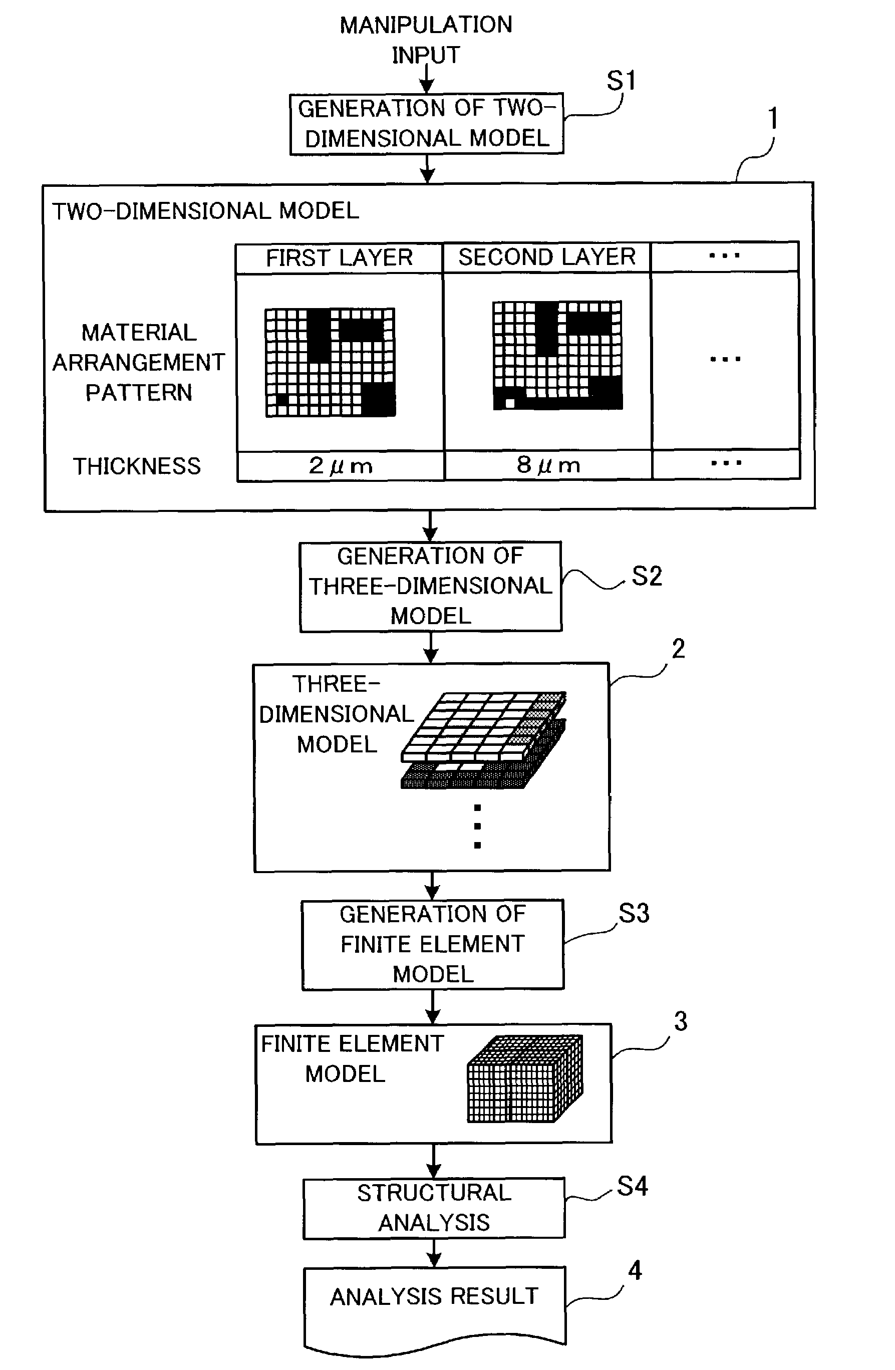
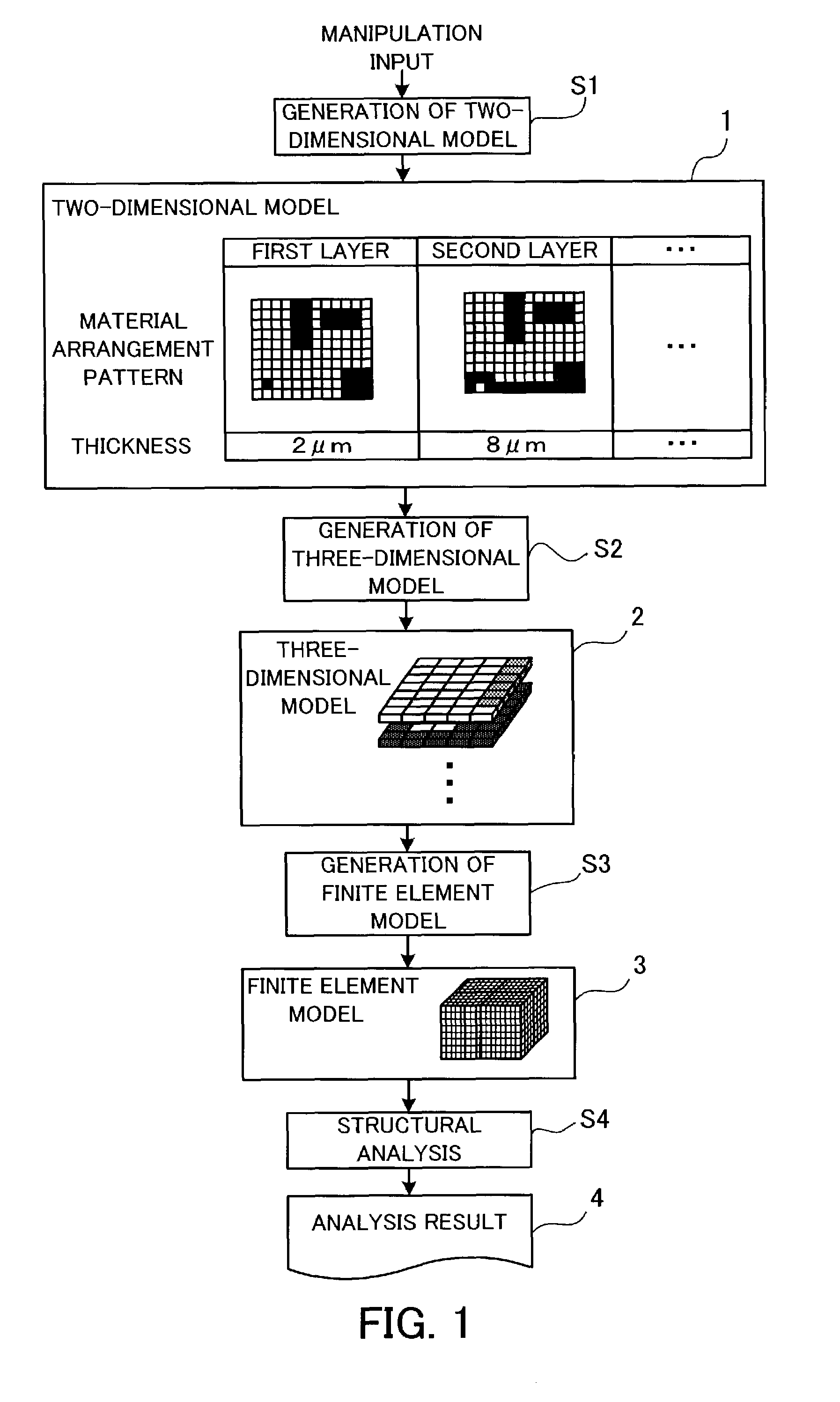
[0076]The first embodiment is explained below. In the first embodiment, a three-dimensional structure of an LSI is generated based on a two-dimensional structure definition of the LSI, and a structural analysis is performed in the three-dimensional space.

[0077]FIG. 4 is a diagram illustrating an example of a hardware construction of a computer which can execute a structural analysis program. The entire system of the computer 100 is controlled by a CPU (central processing unit) 101. A RAM (random access memory) 102, an HDD (hard disk drive) 103, a graphic processing unit 104, an input interface 105, and a communication interface 106 are connected to the CPU 101 through a bus 107.

[0078]The RAM 102 temporarily stores at least portions of an operating system (OS) and an application program executed by the CPU 101, as well as various data which are necessary for execution of the programs by the CPU 101. The HDD 103 stores the operating system (OS) and the application program such as a st...

second embodiment

[0333]Next, the second embodiment is explained. In the second embodiment, an LSI is produced, where the structural strength of the LSI is verified by using the functions of the structural analysis apparatus in the first embodiment.

[0334]FIG. 35 is a diagram illustrating an example of an LSI manufacturing system. In the example of FIG. 35, the LSI manufacturing system is constituted by a circuit design apparatus 810, a production control apparatus 820, and a plurality of semiconductor production apparatuses 831, 832, 833, ááá, where the plurality of semiconductor production apparatuses 831, 832, 833, ááá are arranged in a semiconductor factory 830. The circuit design apparatus 810 and the plurality of semiconductor production apparatuses 831, 832, 833, ááá are connected to the production control apparatus 820.

[0335]The circuit design apparatus 810 is a computer provided for designing circuits of LSIs. The circuit design apparatus 810 has the functions (including layout design and str...

example of application

[0350]The processing functions indicated in the first and second embodiments can be realized by computers. In this case, programs which describe details of processing realizing the functions which the structural analysis apparatus, the circuit design apparatus, and the production control apparatus should have are provided. When the computers execute the programs, the above processing functions are realized on the computers. The programs describing the details of processing can be stored in a computer-readable storage mediums. The computer-readable storage mediums may be a magnetic storage device, an optical disk, an optical magnetic recording medium, a semiconductor memory, or the like. The magnetic storage device may be a hard disk device (HDD), a flexible disk (FD), a magnetic tape, or the like. The optical disk may be a DVD (Digital Versatile Disk), a DVD-RAM (Random Access Memory), a CD-ROM (Compact Disk Read Only Memory), a CD-R (Readable) / RW (ReWritable), or the like. The opti...


PUM


Abstract

A structural analysis program which enables easy structural analysis in accordance with a finite element method based on data representing a two-dimensional shape. A two-dimensional model of a structure is produced in response to a manipulation input which designates a material arrangement pattern and a thickness of each layer of the structure. A three-dimensional model is produced by adding the designated thickness of each layer to the material arrangement pattern of the layer so as to make the material arrangement pattern three-dimensional and stacking the three-dimensionalized material arrangement pattern of each layer. A finite element model is produced by dividing the three-dimensional model into a plurality of voxels. The computer performs structural analysis based on the produced finite element model. Thereby, an analysis result of a multilayer structure defined by the two-dimensional model is obtained.

Description

BACKGROUND OF THE INVENTION[0001]1) Field of the Invention[0002]The present invention relates to a structural analysis program, a structural analysis method, and a structural analysis apparatus which are provided for performing a structural analysis of physical properties, and a production process of a semiconductor integrated circuit which undergoes a structural analysis in a design stage. The present invention relates in particular to a structural analysis program, a structural analysis method, and a structural analysis apparatus which are provided for performing a structural analysis by using a finite element model, and a production process of a semiconductor integrated circuit which undergoes a structural analysis using a finite element model in a design stage.[0003]2) Description of the Related Art[0004]In the field of the computer graphics (CG), a space is divided into voxels. The voxels are each a very small hexahedral element constituting the space. The voxel technique is us...

Claims


Application Information

Patent Timeline
Patent Type & Authority Patents(United States)
IPC IPC(8): G06F17/50G06F19/00
CPCG06F17/5018G06F30/23
Inventor AMAKAI, MAKOTOSUGIURA, IWAONEGISHI, TAKANORIKAWASHIMA, YASUHIROKAMURAI, GENIMAMURA, KAZUYUKI
Owner FUJITSU SYST EAST
Why Eureka
Try Eureka