Alignment of clock signal with data signal

a clock signal and data signal technology, applied in the direction of digital transmission, channel dividing arrangement, baseband system details, etc., can solve the problems of area and power consumption versus speed, and achieve reliable clock-data alignment, low power consumption, and reduced power consumption

Inactive Publication Date: 2009-02-03
ALTERA CORP
View PDF38 Cites 21 Cited by
  • Summary
  • Abstract
  • Description
  • Claims
  • Application Information

AI Technical Summary

Benefits of technology

[0007]The present invention achieves reliable clock-data alignment, with reduced power consumption, in synchronous applications, where the clock is sent with the data and the factors that give rise to clock-data misalignment are substantially constant during operation. Thus, e.g., if the only factor giving rise, in a particular synchronous application, to clock-data misalignment is path length differences between the clock path and the data path or paths, the invention can achieve clock-data alignment with low power consumption. Even if the “constant” factors are different each time the device is powered on, the invention will achieve the desired result.
[0010]In either of the foregoing embodiments (and their variants), each data receiving circuit preferably has its own clock recovery circuit for both asynchronous operation and for training in synchronous operation. Preferably, there is only one separate comparison circuit (preferably a loop circuit as described) for comparing each respective recovered clock to the received clock. That one comparison circuit is used to adjust one delay line at a time sequentially, until all delay lines have been adjusted. However, it is also possible to provide a separate comparison circuit associated with each delay line. These comparison circuits could then operate simultaneously if desired. The tradeoff is one of area and power consumption versus speed. However, each comparison and delay determination is relatively fast, and sequential operation with a single circuit is not expected to lengthen the training cycle so much as to make the cost in area and power consumption of multiple comparison circuits worthwhile in most applications.

Problems solved by technology

The tradeoff is one of area and power consumption versus speed.
However, each comparison and delay determination is relatively fast, and sequential operation with a single circuit is not expected to lengthen the training cycle so much as to make the cost in area and power consumption of multiple comparison circuits worthwhile in most applications.

Method used


Image

  • Alignment of clock signal with data signal
  • Alignment of clock signal with data signal
  • Alignment of clock signal with data signal

Examples


second embodiment

[0026]In a second embodiment, the received clock branches to each data path (as it would be expected to do in any embodiment), and the variable delay lines are present in the individual clock branches, so that the received clock can be delayed by different amounts for each data path. In a variant of this embodiment, delays are also present in the data paths, so that if the received clock lags any data signal, that signal can be delayed, rather than further delaying the received clock by the complementary phase amount.

[0027]Regardless of which of the foregoing embodiments, and the respective variants thereof, is used, there also are two different embodiments with respect to the comparison circuitry that compares the recovered clock for each data signal with the received clock to determine the respective delay value for that data signal or its clock input. In one embodiment, a comparison circuit is provided for each data receiving circuit. This allows all of the delays to be determine...

first embodiment

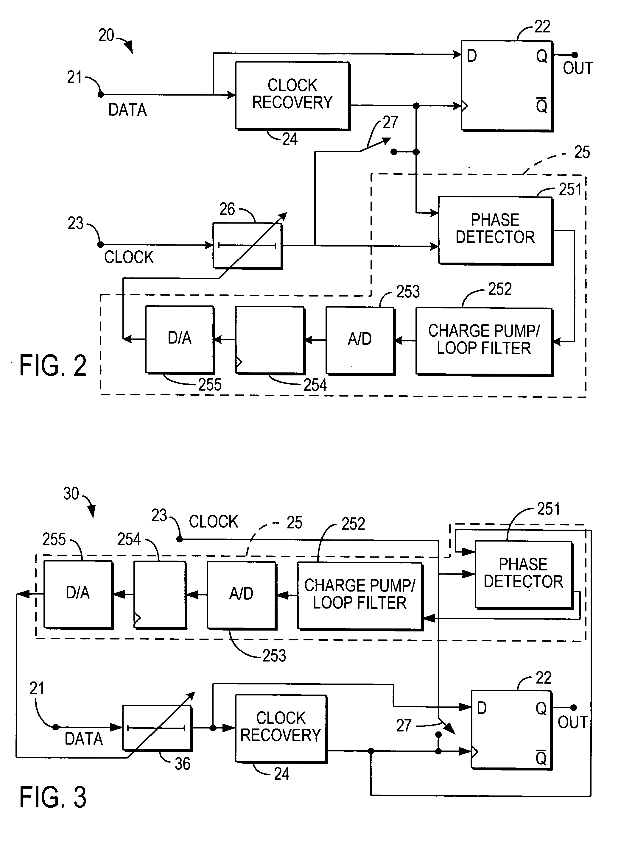
[0031]FIG. 2 shows a data receiving circuit 20 incorporating the present invention. Circuit 20 includes a data input 21 and a decision circuit 22, which may be as simple as a D-type flip flop, to which data input 21 is connected and which is meant to be clocked either by a clock sent with the incoming data signal and received at clock input 23 (synchronous operation), or by a clock recovered from the incoming data themselves by clock recovery circuitry 24 (asynchronous operation).

[0032]In the training mode of synchronous operation, in accordance with the present invention, comparison circuit 25, which preferably is loop circuit similar to a phase-locked loop or delay-locked loop, and incorporating a phase detector 251 and a charge pump and loop filter 252, adjusts variable delay line 26. Optionally, analog-to-digital converter 253, register 254 and digital-to-analog converter 255 are provided so that the delay value of variable delay line 26 can be stored and used as described below...

embodiment 40

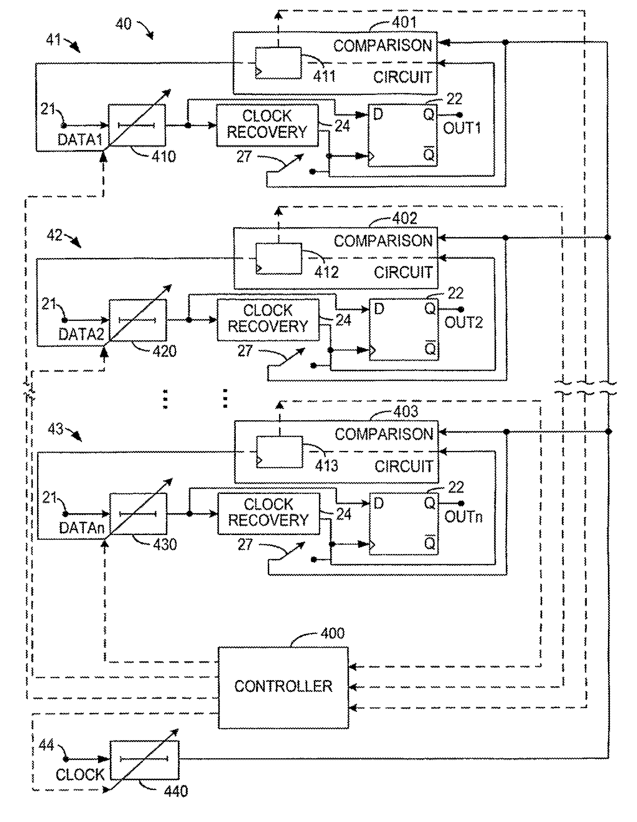
[0035]The multiple channel case (likely to be more common) is shown in FIGS. 4 and 5. In embodiment 40 shown in FIG. 4, each channel—i.e., each data receiving circuit 41-43—includes clock recovery circuitry 24, allowing use of that channel in an asynchronous system. A single received clock 44 is also available in a synchronous system. It should be noted that there may be more than one received clock, each associated with one or more received data channels. However, each group of one received clock and its associated data channels may be considered a single multiple channel receiver in accordance with this invention.

[0036]For use in a synchronous system, each data receiving circuit 41-43 has a respective variable delay line 410, 420, 430 on its input. Each of those variable delay lines is controlled by, and part of, a comparison circuit 401, 402, 403, each similar to comparison circuit 25 of FIGS. 2 and 3, that compares the received clock to the recovered clock and delays the respect...


PUM


Abstract

A received clock signal is aligned (“eye centered”) with a received data signal by recovering a separate clock from the data signal and comparing and aligning the received clock with the recovered clock by delaying one or both of the received clock and the received data as necessary. After the necessary delays are set, the comparison / alignment circuitry can be turned off, until the next time alignment is necessary, to conserve power. In a multiple channel system, any combination of each received data channel, the received clock, or individual branches of the received clock in each channel can be delayed as necessary. Each channel can have its own comparison / alignment circuitry so that all channels can be aligned simultaneously, or re-usable circuitry can be provided for connection sequentially to each channel where sequential alignment of the channels is fast enough.

Description

BACKGROUND OF THE INVENTION[0001]This invention relates to the alignment of a received clock signal with a received data signal. More particularly, this invention relates to such alignment on a programmable logic device.[0002]It is almost axiomatic that digital systems are clocked. For a clock of period T, the clock signal is typically a series of square (or rectangular) pulses of durations T / 2, separated by zero-amplitude intervals of durations T / 2. Such a clock has a rate or frequency of 1 / T. The clock is used to time data signals, with each data pulse having a duration T. However, there is no reason why consecutive data pulses need be separated by zero-amplitude intervals. Therefore, two or more (n) consecutive data pulses can be transmitted as a single continuous “high” signal of duration nT. In each clock period T, one data pulse can be transmitted. Thus, the data rate of the system is the same as that of the clock rate. In a double data rate system, data is sampled on both ris...

Claims


Application Information

Patent Timeline
Patent Type & Authority Patents(United States)
IPC IPC(8): H04L7/00H03D3/24
CPCH04L7/033H04L25/14H04L7/0037H04L7/0041
Inventor KWASNIEWSKI, TADBEREZA, BILLWANG, SHOUJUNBAIG, MASHKOORMEI, HAITAO
Owner ALTERA CORP
Why Eureka
Try Eureka