Supercharge Your Innovation With Domain-Expert AI Agents!

Semiconductor structure having a strained region and a method of fabricating same

a technology of semiconductors and regions, applied in the direction of semiconductor/solid-state device manufacturing, semiconductor devices, electrical devices, etc., can solve the problems of compromising advantages, affecting reliability, and affecting the performance of the ultimate transistor, so as to achieve enhanced performance and low defects

Inactive Publication Date: 2009-02-24
TAIWAN SEMICON MFG CO LTD
View PDF36 Cites 1 Cited by
  • Summary
  • Abstract
  • Description
  • Claims
  • Application Information

AI Technical Summary

Benefits of technology

The structure maintains high electron and hole mobility while reducing deleterious effects from sharp trench corners, resulting in enhanced performance and reliability of strained channel transistors by using rounded corners and appropriate lattice mismatched layers.

Problems solved by technology

Moreover, ion implantation procedures typically used in MOSFET fabrication may damage the strained layers, thereby compromising the advantages that might otherwise be realized from the presence of the strained material.
Studies of prior art devices and their methods of fabrication generally have shown that sharp (˜90°) top and bottom corners of isolation trenches with vertical or near vertical sidewalls are deleterious to the reliability of transistors such as MOSFETs, as well as other electrical devices, that incorporate them.

Method used


Image

  • Semiconductor structure having a strained region and a method of fabricating same
  • Semiconductor structure having a strained region and a method of fabricating same
  • Semiconductor structure having a strained region and a method of fabricating same

Examples


Embodiment Construction

[0016]The making and using of the presently preferred embodiments are discussed in detail below. It should be appreciated, however, that the present invention provides many applicable inventive concepts that can be embodied in a wide variety of specific contexts. The specific embodiments discussed are merely illustrative of specific ways to make and use the invention, and do not limit the scope of the invention.

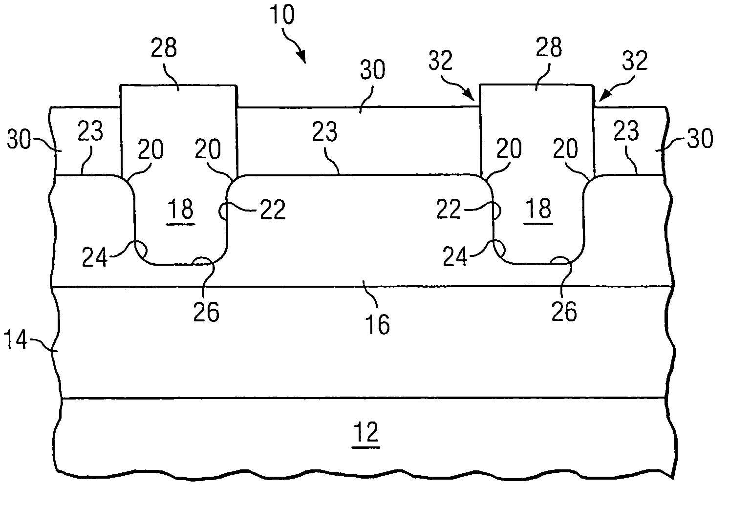
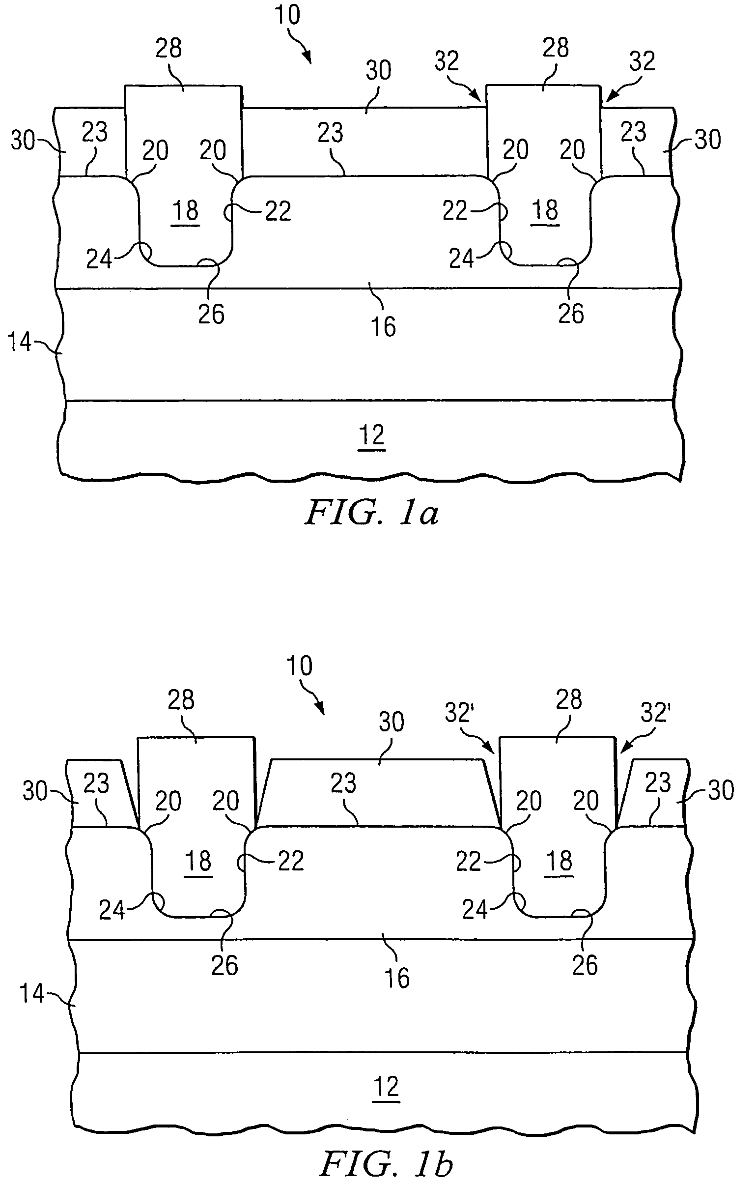
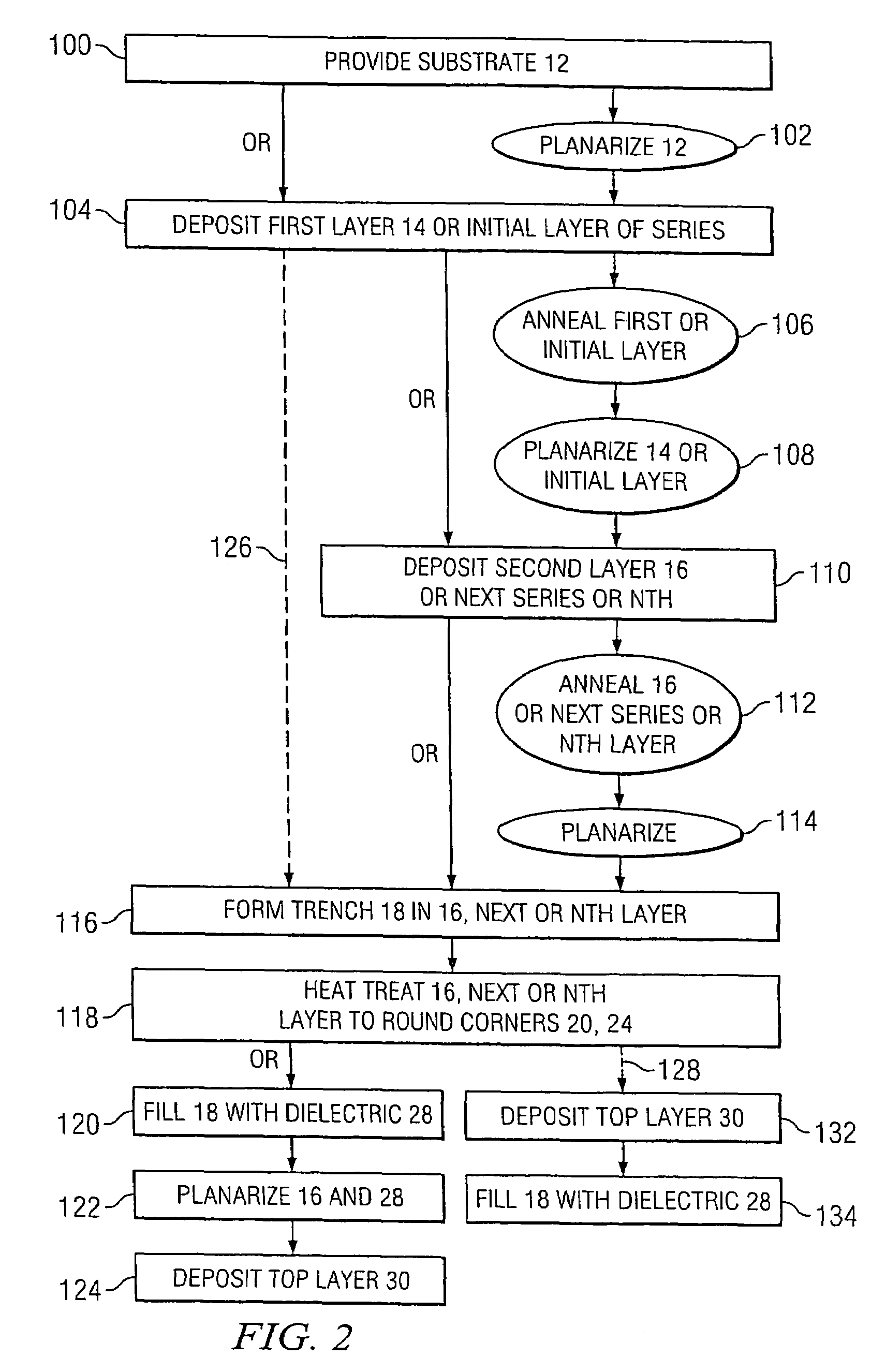
[0017]A preferred embodiment of the present invention includes a semiconductor substrate, which may be a semiconductor body or a semiconductor stratum on a subjacent body. A preferred material of the semiconductor substrate is silicon. A first epitaxial crystalline layer is formed, as by deposition, on a free surface of the substrate. The first layer is preferably Si, Ge, C or a compound semiconductor, such as SiGe. In addition, it is preferred that the first layer be Si-rich or Ge-rich. The first layer may be produced by a multi-step deposition process in a single chamber or...


PUM


Abstract

A semiconductor structure including a highly strained selective epitaxial top layer suitable for use in fabricating a strained channel transistor. The top layer is deposited on the uppermost of a series of one or more lower layers. The lattice of each layer is mismatched with the lattice of its subjacent layer by an amount not less than the lattice mismatch between the lowest layer of the series and a substrate on which it resides. A trench is formed in the uppermost series layer. The trench has rounded corners so that a dielectric material filling the trench conforms to the round corners. The rounded corners are produced by heating the uppermost series layer after trench formation.

Description

[0001]This application is a divisional of patent application Ser. No. 10 / 657,616 entitled “SEMICONDUCTOR STRUCTURE HAVING A STRAINED REGION AND A METHOD OF FABRICATING SAME,” filed on Sep. 8, 2003, now U.S. Pat. No. 7,045,836 which application is incorporated herein by reference.TECHNICAL FIELD[0002]The present invention relates to a semiconductor structure having a strained region, the structure being usable for the fabrication of a strained channel semiconductor transistor or other device, and to a method of fabricating such a structure.BACKGROUND[0003]It has been known for some time that high electron and hole mobility in transistors, such as MOSFETs, may be achieved through the use of strained silicon or other layers epitaxially grown on relaxed SiGe or other layers. It has been demonstrated that the strained layers are eminently suitable as channel regions of transistors such as MOSFETs, and result in devices having enhanced performance. It has also been shown that strained lay...

Claims


Application Information

Patent Timeline
Patent Type & Authority Patents(United States)
IPC IPC(8): H01L31/0368
CPCH01L21/76232H01L29/78H01L29/7846H01L21/02381H01L21/02529H01L21/02532H01L21/0262H01L21/02639
Inventor LEE, WEN-CHINGE, CHUNG-HUHU, CHENMING
Owner TAIWAN SEMICON MFG CO LTD
Features
  • R&D
  • Intellectual Property
  • Life Sciences
  • Materials
  • Tech Scout
  • Unparalleled Data Quality
  • Higher Quality Content
  • 60% Fewer Hallucinations
Learn More