

Semiconductor lead frame, semiconductor package having the same, and method of plating the same
a semiconductor and lead frame technology, applied in the direction of fixed capacitors, variable capacitors, fixed capacitor details, etc., can solve the problems of ineffective conventional methods for reducing whiskers when using cu substrates, malfunctions of electronic components, and generation of whiskers, so as to reduce grain size, reduce plating time, and reduce the effect of grain siz
- Summary
- Abstract
- Description
- Claims
- Application Information
AI Technical Summary
Benefits of technology
Problems solved by technology
Method used
Image

Examples
Embodiment Construction
[0035]The present invention will now be described more fully with reference to the accompanying drawings in which exemplary embodiments of the invention are shown.
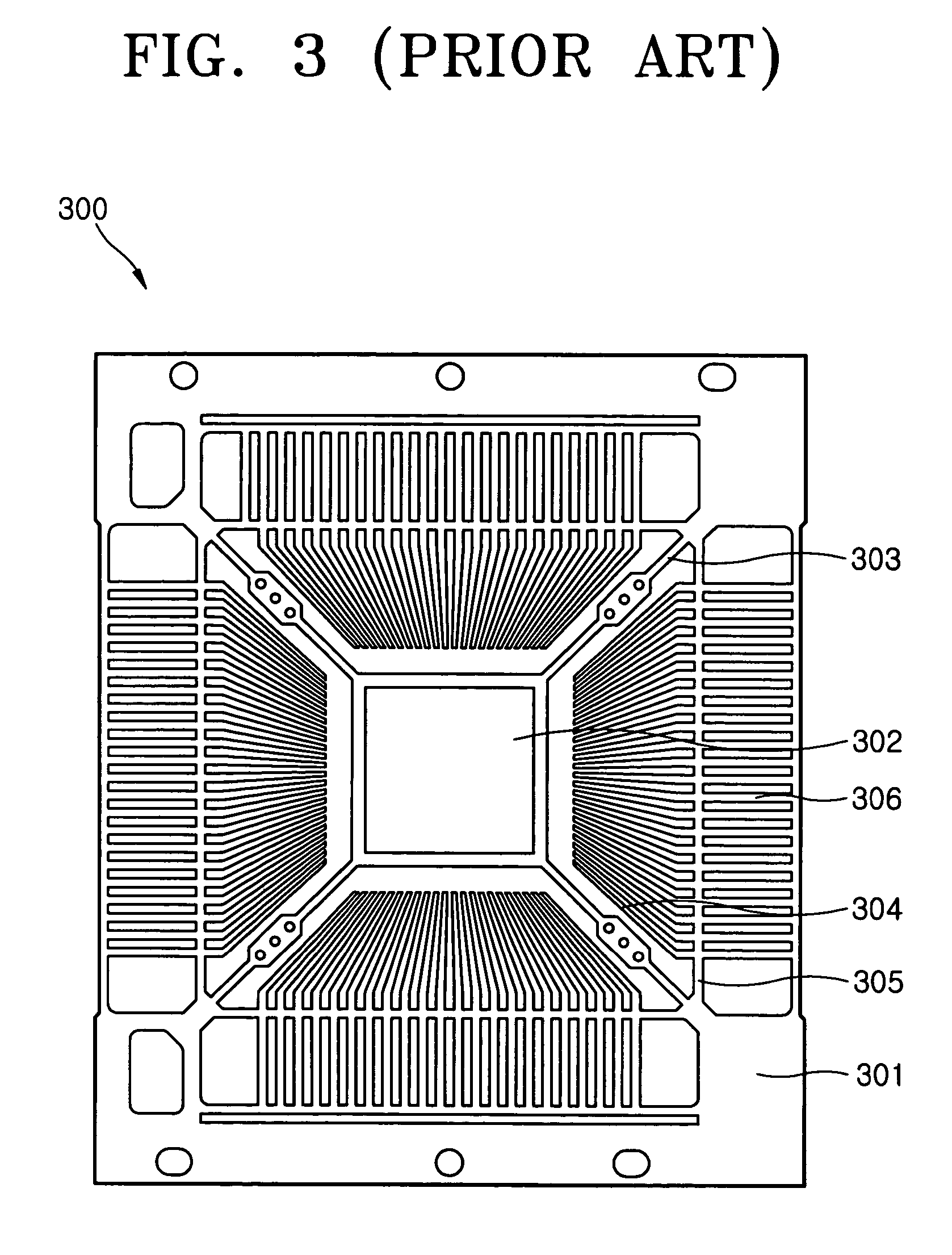
[0036]FIG. 3 is a top view of a semiconductor lead frame 300 according to an embodiment of the present invention.
[0037]Referring to FIG. 3, the semiconductor lead frame 300 comprises a die pad 302 on which a semiconductor chip is mounted. The die pad 302 is disposed at the center of a plate 301, and corners of the die pad 302 are supported by tie bars 303.
[0038]A plurality of leads 304 is disposed on edges of the die pad 302. The leads 304 are adjacently connected to a dambar 305. Wire bonding regions to be connected to terminals of a semiconductor chip to be mounted in a subsequent process are formed on edges of the leads 304. External connection leads 306 are formed on opposite sides of the dambar 305 from the leads 304 and enable the leads 304 to be connected to external terminals when the semiconductor lead frame 300 i...
PUM
| Property | Measurement | Unit |
|---|---|---|
| size | aaaaa | aaaaa |
| length | aaaaa | aaaaa |
| length | aaaaa | aaaaa |
Abstract
Description
Claims
Application Information