Surface acoustic wave element, surface acoustic wave device, duplexer, and method of making surface acoustic wave element

a surface acoustic wave and element technology, applied in the field of surface acoustic wave elements, surface acoustic wave devices, duplexers, etc., can solve the problems of difficult to control the thickness of the undercoat layer, difficult to control the doping depth of the substrate surface likewise, and the character of deterioration, etc., to achieve uniform electric charge distribution, low volume resistivity, and volume resistivity of the piezoelectric substrate

Active Publication Date: 2009-03-17
SNAPTRACK
View PDF13 Cites 8 Cited by
  • Summary
  • Abstract
  • Description
  • Claims
  • Application Information

AI Technical Summary

Benefits of technology

[0011]This surface acoustic wave element comprises a piezoelectric substrate having a low volume resistivity, whereas the volume resistivity is not more than 1.5×10¹⁴ Ω·cm. The inventors have newly found that a uniform electric charge distribution is achieved when the volume resistivity of the piezoelectric substrate is as low as such, even under conditions where a uniform electric charge distribution occurs in a conventional substrate whose volume resistivity is 1015 Ω·cm or more. Thus, the occurrence of discharging between IDT electrodes is suppressed in this surface acoustic wave element, whereby characteristics are significantly restrained from deteriorating. Also, since the volume resistivity of the piezoelectric substrate is not less than 3.6×10¹⁰ Ω·cm, IDT electrodes are significantly kept from short-circuiting with each other.
[0012]Preferably, the piezoelectric substrate is doped with at least one species of dopants among Fe, Mn, Cu, and Ti. The selection of the dopants mentioned above can lower the volume resistivity of the piezoelectric substrate.
[0015]Preferably, the DT electrode is constituted by Al or an Al alloy having a high orientation. This allows the IDT electrode to have a high electric power resistance.
[0017]This surface acoustic wave device comprises a piezoelectric substrate having a low volume resistivity, whereas the volume resistivity is not more than 1.5×10¹⁴ Ω·cm. The inventors have newly found that a uniform electric charge distribution is achieved when the volume resistivity of the piezoelectric substrate is as low as such, even under conditions where an uneven electric charge distribution occurs in a conventional substrate whose volume resistivity is 1015 Ω·cm or more. Thus, the occurrence of discharging between IDT electrodes is suppressed in this surface acoustic wave device, whereby characteristics are significantly restrained from deteriorating. Also, since the volume resistivity of the piezoelectric substrate is not less than 3.6×10¹⁰ Ω·cm, IDT electrodes are significantly kept from short-circuiting with each other.
[0019]This duplexer comprises a piezoelectric substrate having a low volume resistivity, whereas the volume resistivity is not more than 1.5×10¹⁴ Ω·cm. The inventors have newly found that a uniform electric charge distribution is achieved when the volume resistivity of the piezoelectric substrate is as low as such, even under conditions where an uneven electric charge distribution occurs in a conventional substrate whose volume resistivity is 1015 Ω·cm or more. Thus, the occurrence of discharging between IDT electrodes is suppressed in this duplexer, whereby characteristics are significantly restrained from deteriorating. Also, since the volume resistivity of the piezoelectric substrate is not less than 3.6×10¹⁰ Ω·cm, IDT electrodes are significantly kept from short-circuiting with each other.

Problems solved by technology

The discharging may melt the IDT electrodes, thereby causing characteristics to deteriorate, such that the frequency characteristic of the device shifts from its desired characteristic, or short-circuiting occurs.
However, the following problem exists in the conventional SAW devices mentioned above.
Namely, it is quite difficult to control the respective thicknesses of the undercoat layer, protective layer, and semiconductor layer formed on the piezoelectric substrate uniformly with a high accuracy.
And, it is quite difficult to control the doping depth of the substrate surface likewise.
Therefore, in many cases, the respective thicknesses of the undercoat layer, protective layer, and semiconductor layer or the doping depth become uneven, and the undercoat layer and the like fail to function sufficiently for homogenizing the electric charge distribution because of this unevenness.
Hence, the conventional SAW devices fail to sufficiently restrain IDT electrodes from melting by discharging.

Method used


Image

  • Surface acoustic wave element, surface acoustic wave device, duplexer, and method of making surface acoustic wave element
  • Surface acoustic wave element, surface acoustic wave device, duplexer, and method of making surface acoustic wave element
  • Surface acoustic wave element, surface acoustic wave device, duplexer, and method of making surface acoustic wave element

Examples


Embodiment Construction

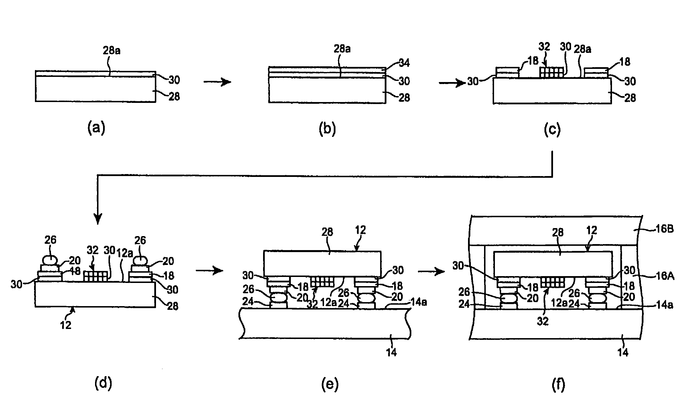
[0032]In the following, modes which are considered the best for embodying the surface acoustic wave element, surface acoustic wave device, duplexer, and method of making the surface acoustic wave element will be explained in detail with reference to the accompanying drawings. Constituents identical or equivalent to each other will be referred to with numerals identical to each other without repeating their overlapping descriptions if any.

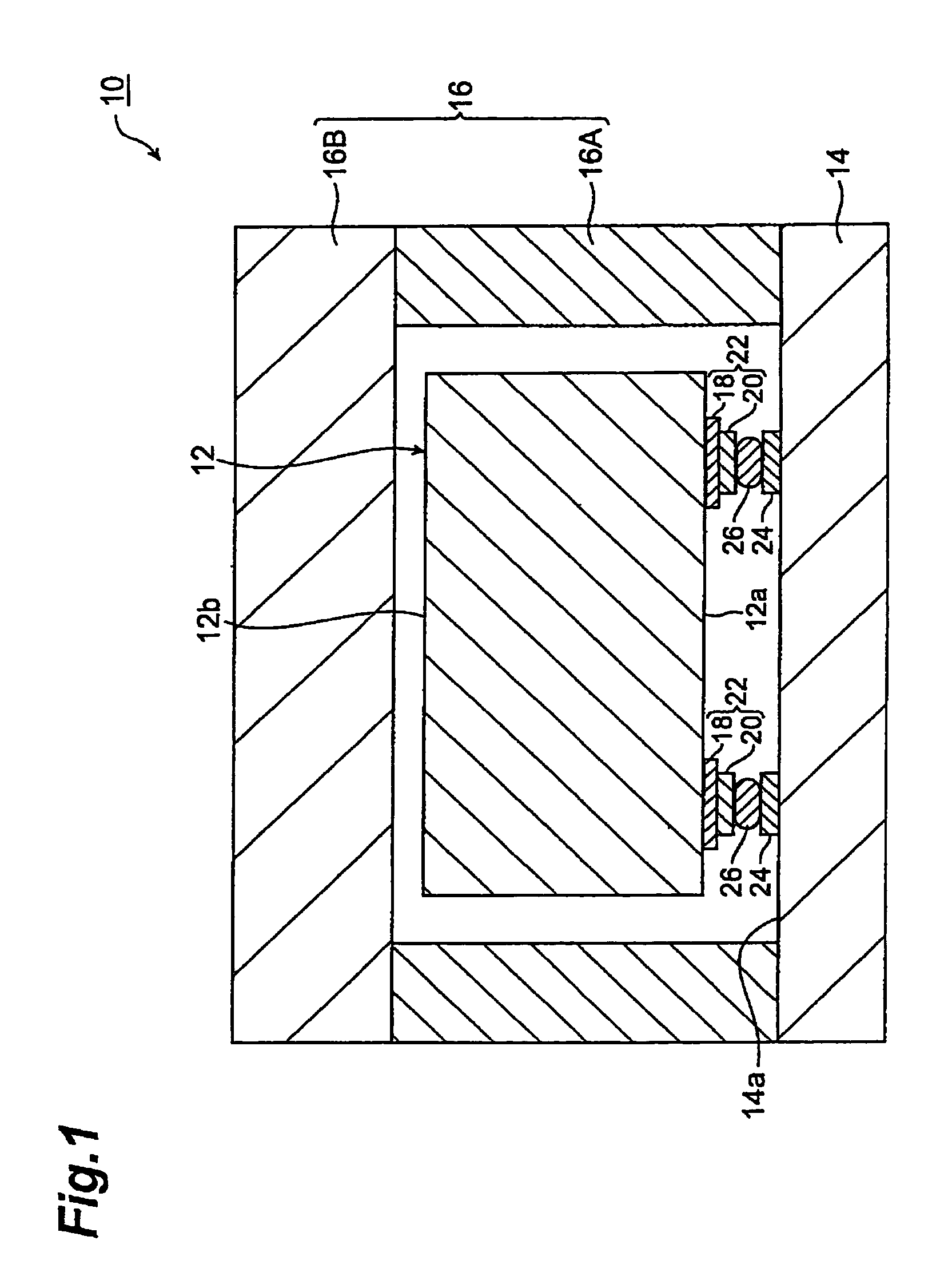
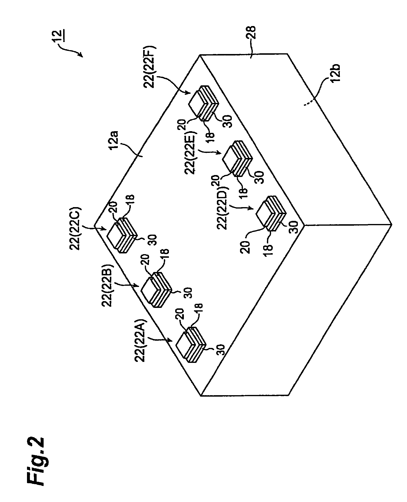
[0033]FIG. 1 is a schematic sectional view of the surface acoustic wave device in accordance with an embodiment of the present invention. As shown in FIG. 1, the surface acoustic wave device (hereinafter referred to as “SAW device”) 10 in accordance with the present invention comprises a surface acoustic wave element (hereinafter referred to as “SAW element”) 12, a mount board 14 for mounting the SAW element 12, and a cover 16 for sealing the SAW element 12. Formed on the lower surface 12a of the SAW element 12 are three pairs of pad electrodes 22 i...


PUM


Abstract

A surface acoustic wave element, a surface acoustic wave device, a duplexer, and a method of making a surface acoustic wave element which significantly restrain characteristics from deteriorating are provided. The surface acoustic wave element in accordance with the present invention comprises a piezoelectric substrate, and an IDT electrode formed on the piezoelectric substrate, whereas the piezoelectric substrate has a volume resistivity of not less than 3.6×10¹⁰ Ω·cm and not more than 1.5×10¹⁴ Ω·cm. This surface acoustic wave element comprises the piezoelectric substrate having a low volume resistivity, whereas the volume resistivity is reduced to 1.5×10¹⁴ Ω·cm or less. Therefore, discharging is restrained from occurring between IDT electrodes, whereby characteristics are significantly kept from deteriorating. Also, since the volume resistivity of the piezoelectric substrate is not less than 3.6×10¹⁰ Ω·cm, the IDT electrodes are significantly prevented from short-circuiting with each other.

Description

BACKGROUND OF THE INVENTION[0001]1. Field of the Invention[0002]The present invention relates to a surface acoustic wave element, a surface acoustic wave device, a duplexer, and a method of making a surface acoustic wave element.[0003]2. Related Background of the Invention[0004]Piezoelectric substrates employed in surface acoustic wave devices (hereinafter referred to as “SAW device”) have been known to have pyroelectric property, thereby generating an uneven electric charge distribution on their surface when heated to 80° C. or higher during a heating process or during their use.[0005]When such an uneven electric charge distribution is generated, a potential difference is caused between a plurality of interdigital transducer electrodes (hereinafter referred to as “IDT electrode”) formed on the substrate, whereby discharging for alleviating the potential difference occurs. The discharging may melt the IDT electrodes, thereby causing characteristics to deteriorate, such that the freq...

Claims


Application Information

Patent Timeline
Patent Type & Authority Patents(United States)
IPC IPC(8): H01L41/08H01L41/18H01L41/22H01L41/09H01L41/29H01L41/39H01L41/41H03H3/08H03H9/02H03H9/10H03H9/145H03H9/25H03H9/72
CPCH03H3/08H03H9/02984H03H9/02992H03H9/0576H03H9/1071H03H9/72H03H9/725H03H9/02921
Inventor SOBU, MASAKIOSANAI, KATSUNORI
Owner SNAPTRACK
Why Eureka
Try Eureka