Differential amplifier circuit and semiconductor device

a technology of amplifier circuit and semiconductor device, which is applied in the direction of differential amplifier, amplifier details, digital storage, etc., can solve the problem of large output voltage error, and achieve the effect of greater

Inactive Publication Date: 2009-03-17
RENESAS ELECTRONICS CORP
View PDF9 Cites 18 Cited by
  • Summary
  • Abstract
  • Description
  • Claims
  • Application Information

AI Technical Summary

Benefits of technology

[0016]When the clock signal CK is inverted in phase, the switches SW1, SW4, SW5 and SW7 are open and the switches SW2, SW3, SW6 and SW8 are closed (shorted), operation is as described above and the output signal is delivered from the output terminal AMPO. That is, the switches SW1, SW4, SW5, SW7 operate in reverse with respect to the switches SW2, SW3, SW6, SW8 and the non-inverted and inverted signals are interchanged in time-shared fashion at the input side (gates of P-channel transistors T3 and T4) and output side (drains of N-channel transistors T9 and T10) in the folded-cascode differential amplifier circuit, thereby enabling an imbalance to be cancelled out.
[0027]Accordingly, as set forth earlier, measures for reducing the input offset voltage Voff have been contemplated. It has been known that the reciprocal of the gain of the differential amplifier circuit is proportional to the input offset voltage, and one example is to make the differential amplifier circuit of the folded-cascode type, which exhibits a high gain. Another method is the chopping technique, which cancels out an imbalance in the threshold value (Vt) of the P-channel transistor T3 and P-channel transistor T4 in the differential stage of the differential amplifier circuit.

Problems solved by technology

A problem with the integrating circuit is that an error ascribable to the input offset voltage of a differential stage in the differential amplifier circuit accumulates in the capacitance of the feedback path, resulting in a larger error in the output voltage.

Method used


Image

  • Differential amplifier circuit and semiconductor device
  • Differential amplifier circuit and semiconductor device
  • Differential amplifier circuit and semiconductor device

Examples


embodiment 1

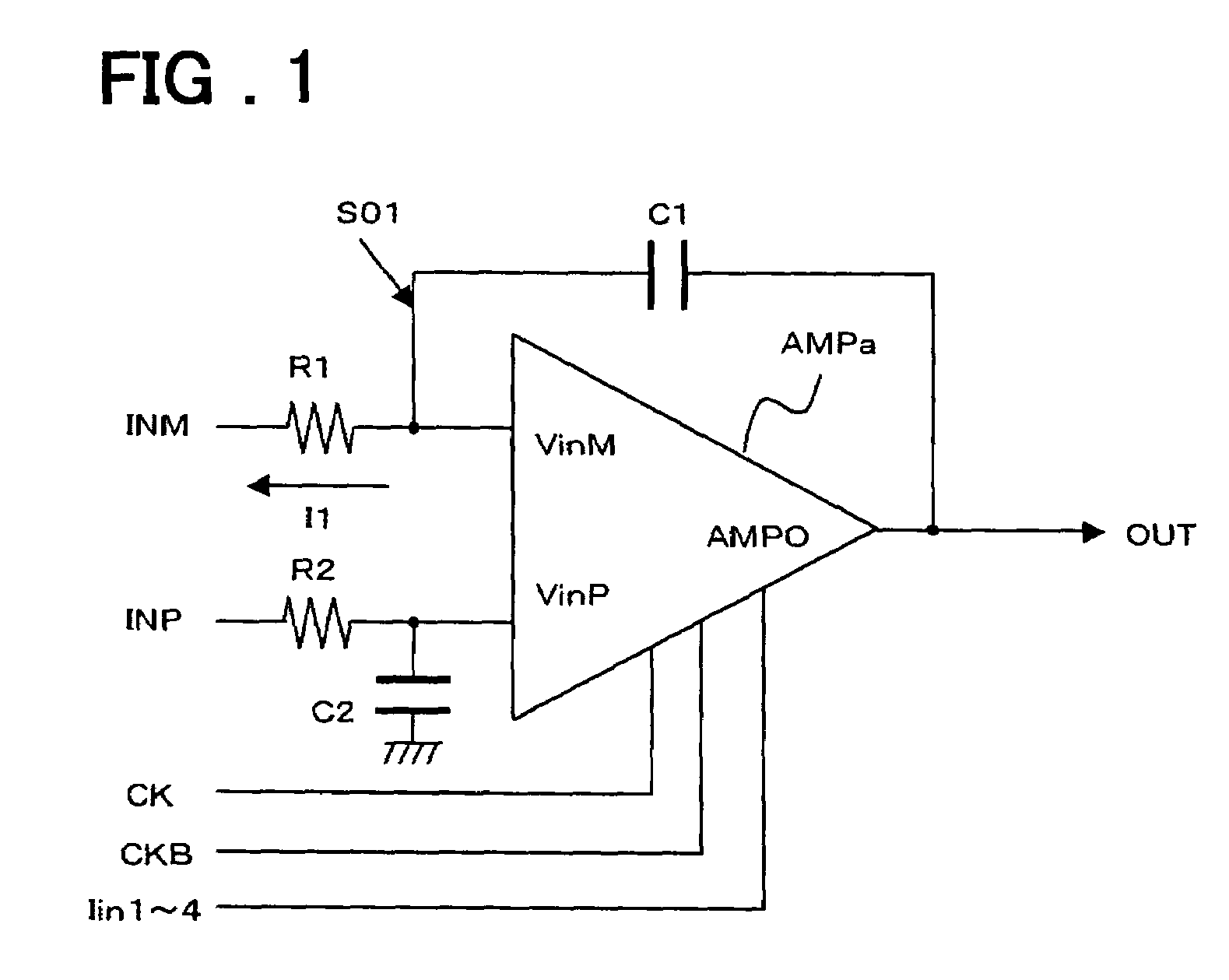
[0069]FIG. 1 is a circuit diagram of an integrating circuit according to this embodiment of the present invention. As shown in FIG. 1, the integrating circuit has a differential amplifier circuit AMPa, resistors R1, R2 and capacitors C1, C2. The form of the connection of the differential amplifier circuit AMPa, resistor R1 and capacitor C1 is the same as that shown in FIG. 6. In order to balance with the resistor R1 and capacitor C1, a dummy resistor R2 and a dummy capacitor C2 whose values are equal to those of the resistor R1 and capacitor C1 are connected between the input terminal INP and non-inverting input terminal VinP and between the non-inverting input terminal VinP and ground GND, respectively.

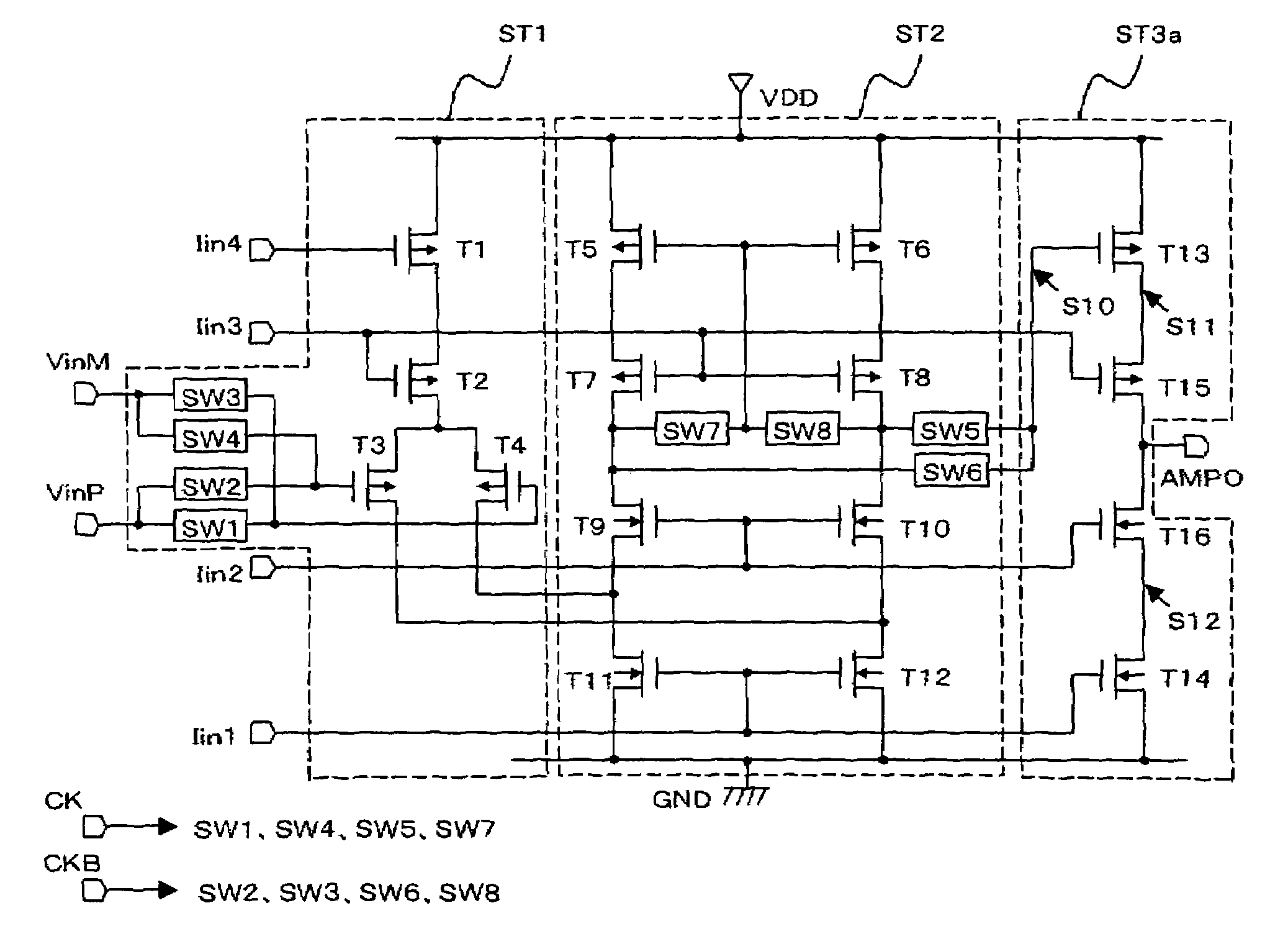
[0070]FIG. 2 is a circuit diagram of a differential amplifier circuit according to this embodiment. Components identical with those shown in FIG. 7 are designated by like reference characters and need not be described again. The differential amplifier circuit of FIG. 2 differs in tha...


PUM


Abstract

A differential amplifier circuit in which an input offset voltage is very small. The differential amplifier circuit includes an input-stage differential amplifier section and a cascode-connected single-ended output section connected to the input-stage differential amplifier section. The input-stage differential amplifier section has a folded-cascode-connection. An inverted signal and non-inverted signal on the input side and output side, respectively, of the input-stage differential amplifier section are switched alternatingly in time-shared fashion by switches that are operated by two chopping clock signals of opposite phase.

Description

FIELD OF THE INVENTION[0001]This invention relates to a differential amplifier circuit and semiconductor device. More particularly, the invention relates to a circuit configuration most suited for application to a highly accurate integrating circuit.BACKGROUND OF THE INVENTION[0002]The accuracy of an output voltage produced by an integrating circuit is affected by the input offset voltage of a differential amplifier circuit used in the integrating circuit. In order to realize a highly accurate integrating circuit, it is necessary to minimize the input offset voltage, which arises due to a variance in the threshold voltage (Vt) and transconductance, etc., of the input transistors of the differential amplifier circuit. A problem with the integrating circuit is that an error ascribable to the input offset voltage of a differential stage in the differential amplifier circuit accumulates in the capacitance of the feedback path, resulting in a larger error in the output voltage. That is, ...

Claims


Application Information

Patent Timeline
Patent Type & Authority Patents(United States)
IPC IPC(8): H03F3/45
CPCG11C7/067G11C7/08H03F3/3022H03F3/393H03F3/45192H03F3/45475H03F3/45775H03F2203/45136H03F2203/45212H03F2203/45512H03F2203/45548H03F2203/45588H03F2203/45616H03F2203/45681H03F2203/45726
Inventor SAITO, HIROFUMI
Owner RENESAS ELECTRONICS CORP
Why Eureka
Try Eureka