
Microelectronic component with foam-metal posts

a microelectronic and foam metal technology, applied in the direction of printed circuits, semiconductor devices, semiconductor/solid-state device details, etc., can solve the problems of increasing the cost of microelectronic packages and the time required for their manufacture, and effectively rigid and unyielding conductive posts,

Active Publication Date: 2009-03-31
TESSERA INC
View PDF12 Cites 5 Cited by
  • Summary
  • Abstract
  • Description
  • Claims
  • Application Information

AI Technical Summary

Benefits of technology

The present invention provides a microelectronic component with conductive posts that have voids and are made from a connected lattice of metal. The conductive posts are offset from support components and can deform when engaging contact pads. The invention also provides a microelectronic package with flexible substrate and conductive posts that are electrically interconnected with the microelectronic component. The conductive posts can deform when engaging a flat surface. The technical effects of the invention include improved electrical connection and flexibility of the microelectronic component.

Problems solved by technology

The modulus of elasticity of the conductive posts, by comparison, is typically about 120 GPa, which means that in such a package the conductive posts are effectively rigid and unyielding.
Further, such an arrangement effectively has no range of plastic deformation because the stress required to achieve plastic deformation of a solid metal pin exceeds values that would likely damage the semiconductor component of a printed circuit board (PCB) to which the structure is mated.
Such narrow tolerances lead to increases in both the cost of the microelectronic packages and the time required for their manufacture.

Method used


Image

  • Microelectronic component with foam-metal posts
  • Microelectronic component with foam-metal posts
  • Microelectronic component with foam-metal posts

Examples


Embodiment Construction

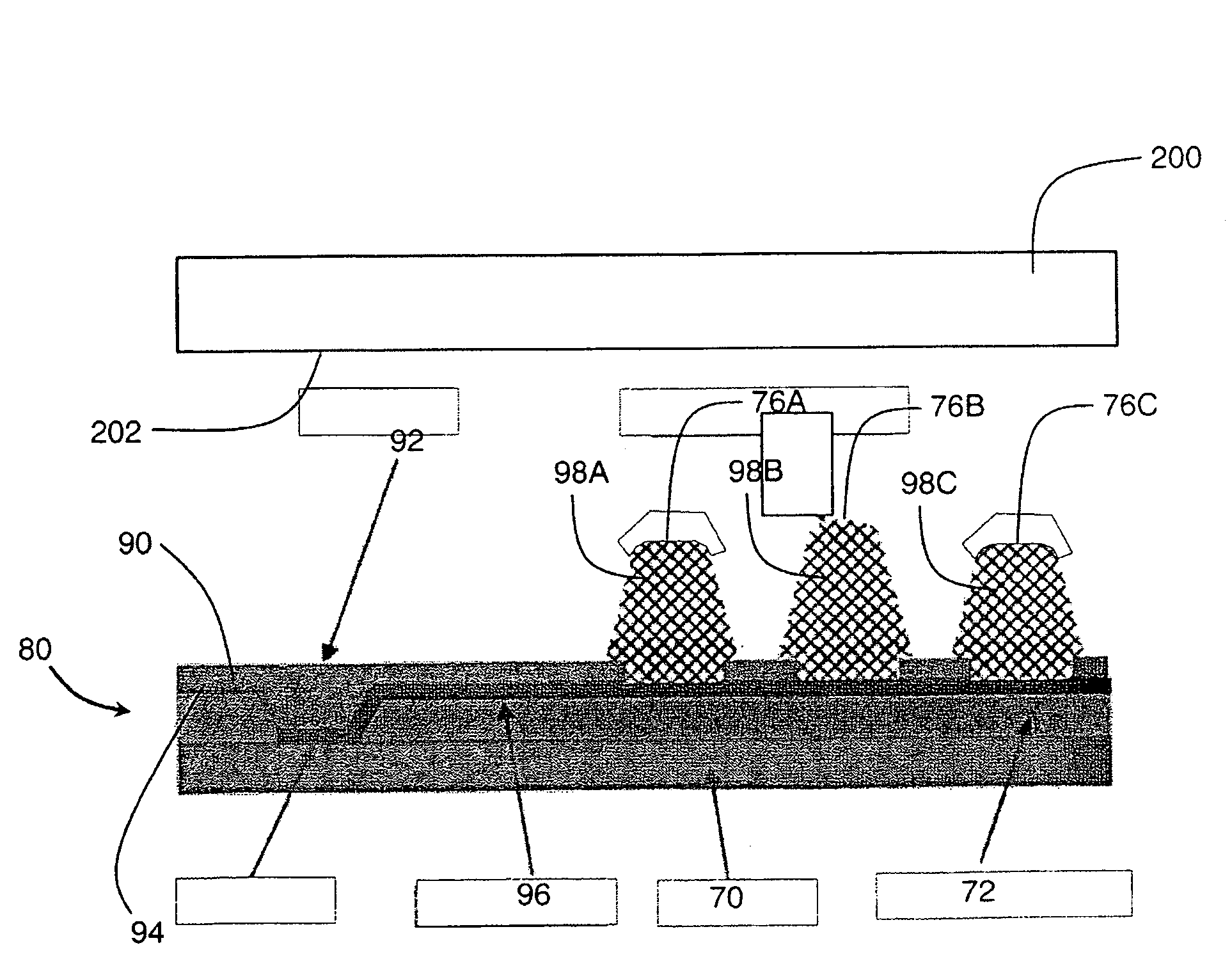
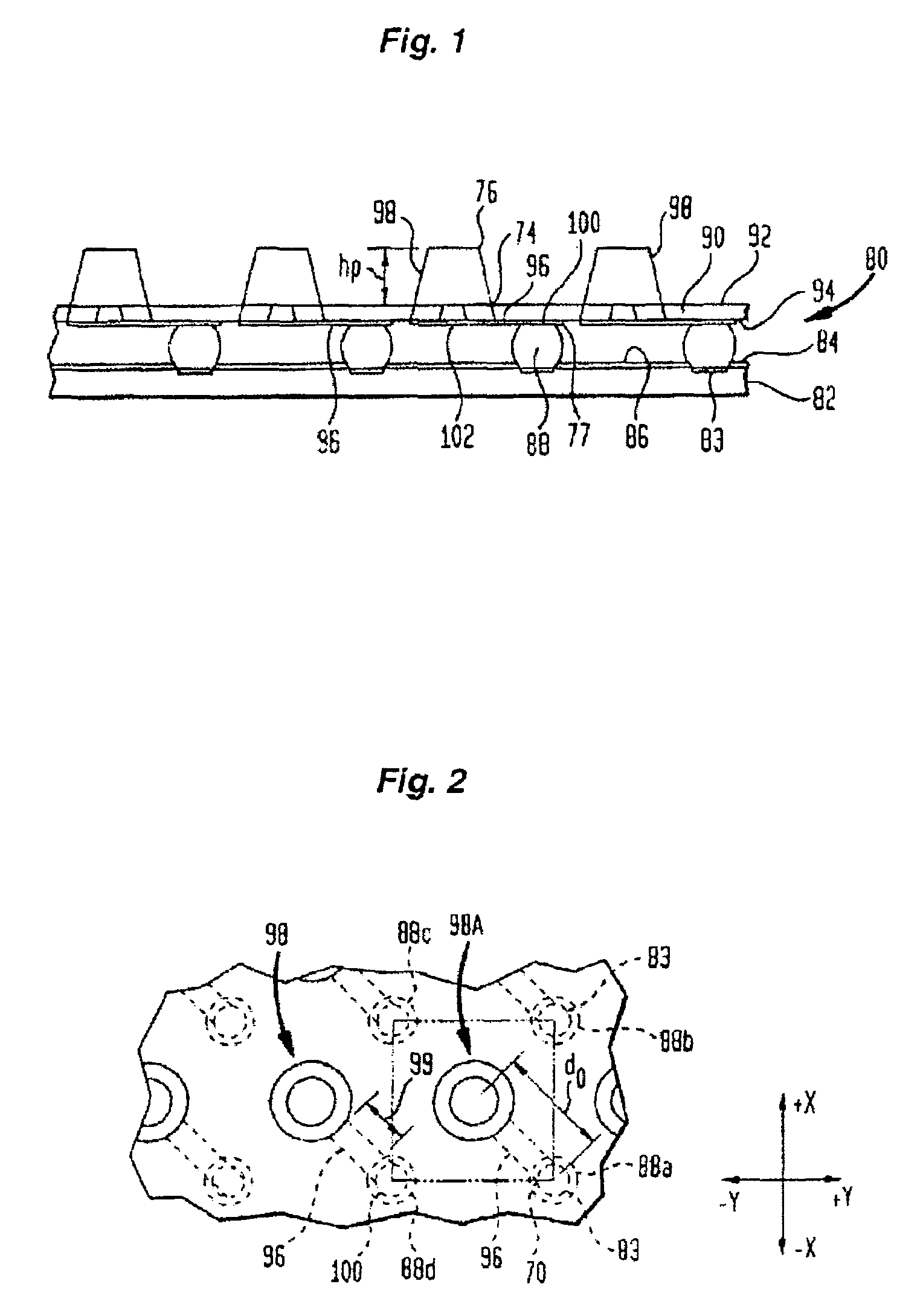
[0021]Referring now to the drawings, wherein like reference numerals represent like elements, there is shown in FIG. 1 a microelectronic package 80, in accordance with one embodiment of the present invention. Microelectronic package 80 includes a microelectronic element, such as a semiconductor chip 82 having a front or contact bearing face 84 and electrical contacts 83 exposed at face 84. A passivation layer 86 may be formed over the contact bearing face 84 with openings at contacts 83.

[0022]The microelectronic package 80 also includes conductive support elements 88 such as solder balls in substantial alignment and electrically interconnected with contacts 83. As best seen in FIG. 2, contacts 83 and support elements 88 are disposed in an array which in this case is a rectilinear grid, having equally spaced columns extending in a first horizontal direction x and equally spaced rows extending in a second horizontal direction y orthogonal to the first horizontal direction. Each contac...


PUM


Abstract

A microelectronic component having a base and a plurality of conductive posts extending from said base. Each of the posts is formed from a connected lattice of metal having voids therein. The lattice may be formed by depositing metal onto a sacrificial element such as an open-celled polymeric foam. During use or during processing, the posts may be deformed , as by crushing the lattice.

Description

BACKGROUND OF THE INVENTION[0001]Semiconductor chips are commonly provided in packages that facilitate handling of the chip during manufacture and during mounting of the chip on an external substrate such as a circuit board or other circuit panel. For example, many semiconductor chips are provided in packages suitable for surface mounting. Numerous packages of this general type have been proposed for various applications. Certain types of packages have been developed which utilize a microelectronic component having a flexible dielectric substrate having conductive traces disposed thereon. In such an arrangement, electrically conductive posts or pillars project from a surface of the flexible substrate. Each post is connected to a portion of one of the traces. This type of microelectronic component is particularly useful in chip packages having arrangements that allow each post to move independently of the other posts. The movement of the posts allows the tips of the plural posts to s...

Claims


Application Information

Patent Timeline
Patent Type & Authority Patents(United States)
IPC IPC(8): H01R12/00
CPCH01L23/49811H01L2924/3011H01L2924/0002H01L2924/00
Inventor HUMPSTON, GILESTHOMPSON, JESSE BURL
Owner TESSERA INC
Learn More