
Non-volatile memory device

a memory device and non-volatile technology, applied in the field of semiconductor memory devices, can solve the problems of deteriorating memory cell efficiency, difficult to determine whether it is the on-cell or the off-cell, and disadvantageous affect with respect to on-cell current, so as to reduce the possibility of read error, improve the current characteristic, and read the effect of relatively fast speed

Active Publication Date: 2009-03-31
SAMSUNG ELECTRONICS CO LTD
View PDF12 Cites 6 Cited by
  • Summary
  • Abstract
  • Description
  • Claims
  • Application Information

AI Technical Summary

Benefits of technology

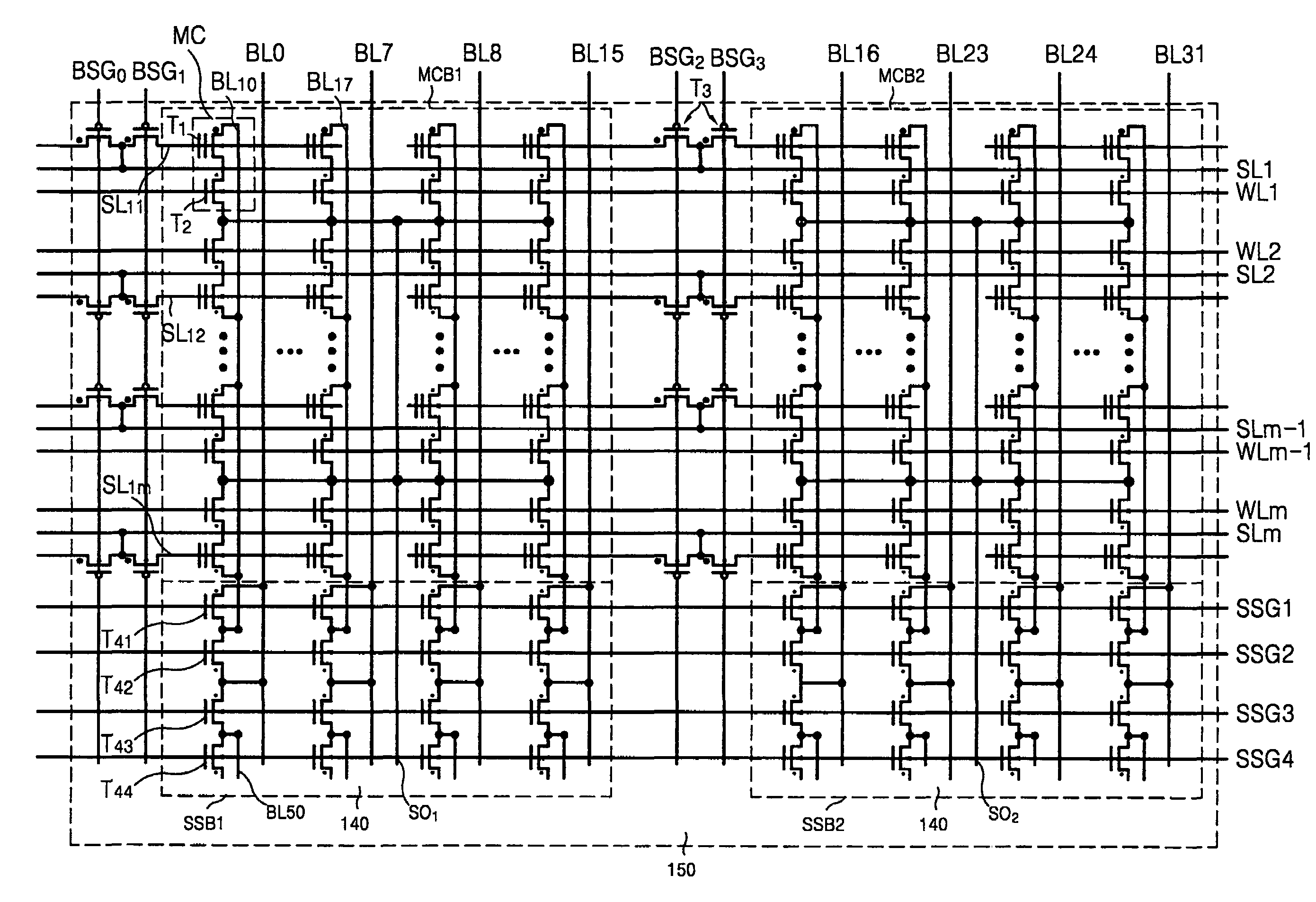
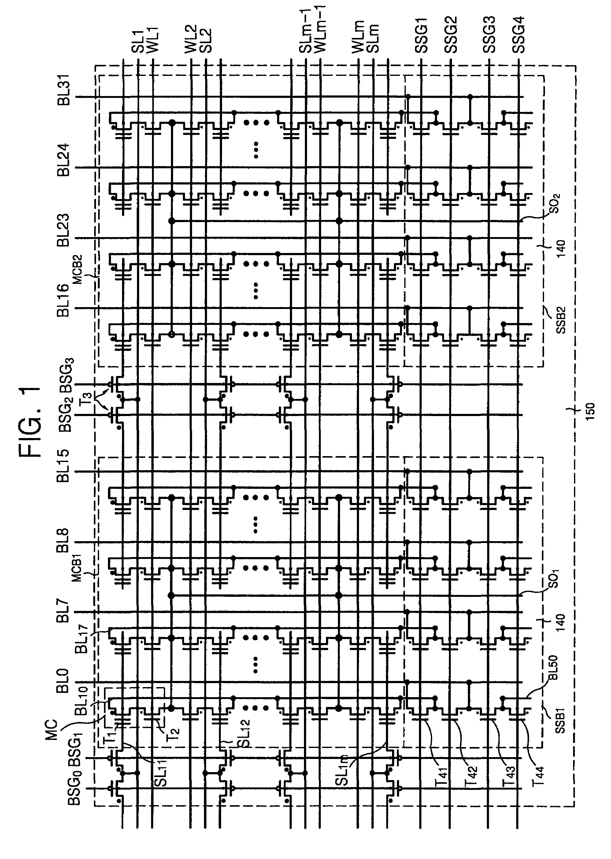
The present invention provides a non-volatile memory device that improves the current characteristic of an EEPROM memory cell to make a read speed faster and reduce the possibility of a read error. The device includes a memory cell block with a plurality of memory cells each having a memory transistor and a selection transistor. A first switching block is configured to selectively connect a global bit line to the local bit line and a second switching block is configured to control the memory cells in the memory cell block in units of a predetermined number of bits. The first switching device can be an NMOS, PMOS, or CMOS device and the predetermined number of bits can be eight bits. The memory cell block can comprise EEPROM memory cells. The second switching device can be a first switching device and a second switching device. The first switching device can selectively connect the global bit line to the local bit line and the second switching device can selectively connect the global sense line to the local sense line. The memory cell block can also include a global sense line and a local sense line for applying a bit line voltage to one of the memory sectors and connecting control gates of the memory transistors in units of a predetermined number of bits. The first switching device can include at least two switching transistors connected in parallel between the global bit line and the local bit line and the second switching device can include at least two switching transistors connected in parallel between the global sense line and the local sense line. The memory cells can include EEPROM memory cells.

Problems solved by technology

As a result, the efficiency in the programming and erasing of the memory cell has been deteriorated.
Consequently, as a threshold voltage of an on-cell memory transistor has increased, the affect with respect to the on-cell current has become disadvantageous.
Accordingly, as the amount of current of the on-cell decreases, it is difficult to determine whether it is the on-cell or the off-cell.
When the determination of the on-cell or off-cell becomes difficult, a read error can occur.
However, this improvement alone has not completely resolved the problem, since various restrictions in view of the process exist.

Method used


Image

  • Non-volatile memory device
  • Non-volatile memory device
  • Non-volatile memory device

Examples


Embodiment Construction

[0027]Hereinafter, aspects of the present invention will be described or explained with reference to the attached figures. The invention is not limited to or by the illustrative preferred embodiments disclosed herein. Like reference numerals in the figures denote like elements.

[0028]It will be understood that, although the terms first, second, etc. may be used herein to describe various elements, these elements should not be limited by these terms. These terms are used to distinguish one element from another, but not to imply a required sequence of elements. For example, a first element can be termed a second element, and, similarly, a second element can be termed a first element, without departing from the scope of the present invention. As used herein, the term “and / or” includes any and all combinations of one or more of the associated listed items.

[0029]It will be understood that when an element is referred to as being “on” or “connected” or “coupled” to another element, it can b...


PUM


Abstract

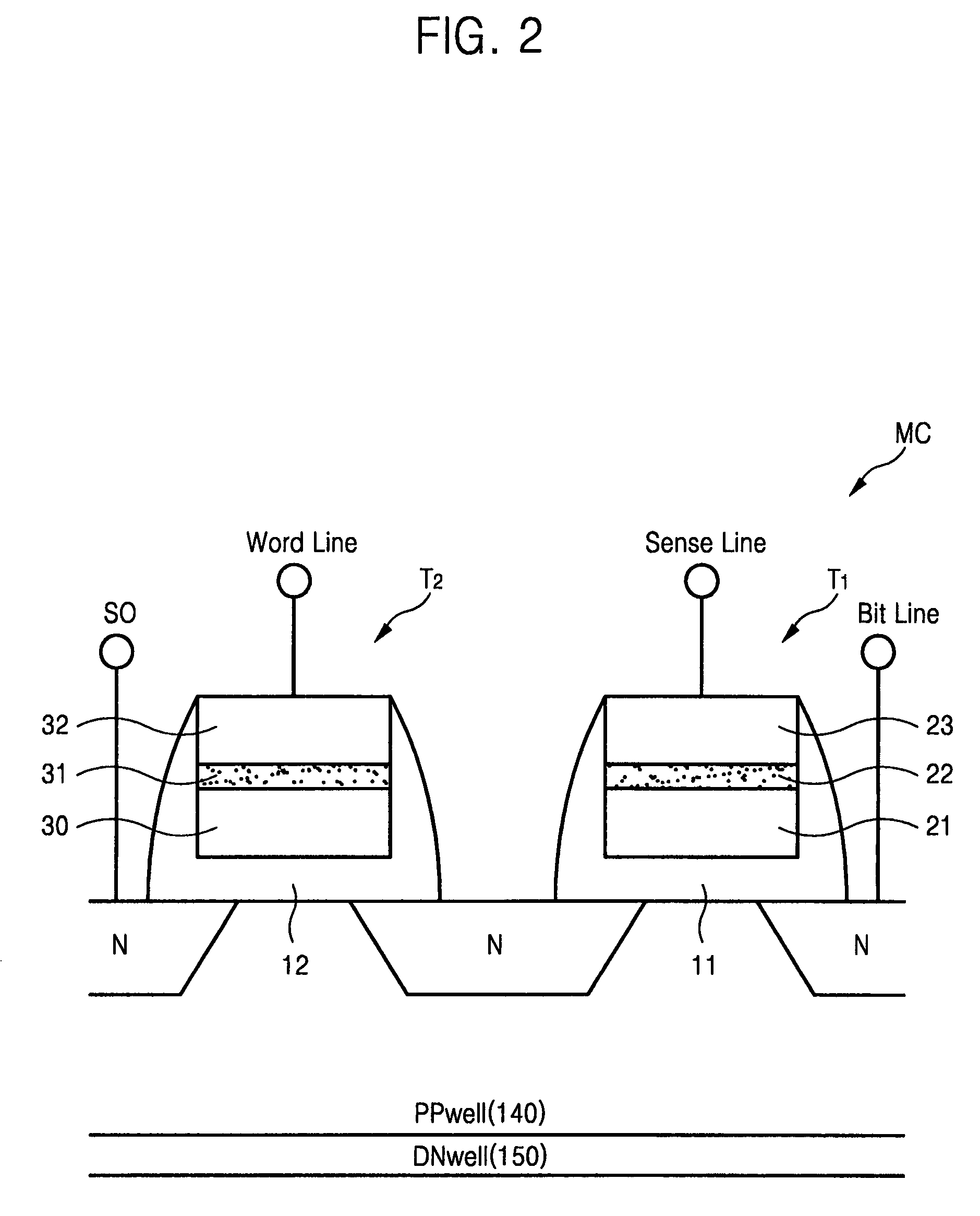
A non-volatile memory device includes a memory cell block, a first switching block, and a second switching block. A plurality of memory cells are arranged in the memory cell block and each of the memory cells includes a memory transistor having a floating gate and a control gate and is connected to a local bit line and includes a selection transistor connected to the memory transistor in series that is connected to a source line. The first switching block selectively connects a global bit line to the local bit line and the second switching block controls the memory cells in the memory cell block in units of a predetermined number of bits. The first switching block includes at least two switching devices connected in parallel between the global bit line and the local bit line.

Description

CROSS-REFERENCE TO RELATED PATENT APPLICATIONS[0001]This application claims the benefit of priority to Korean Patent Application No. 10-2006-0062626, filed on Jul. 4, 2006, in the Korean Intellectual Property Office, the disclosure of which is incorporated herein in its entirety by reference.BACKGROUND OF THE INVENTION[0002]1. Field of the Invention[0003]The present invention relates to a semiconductor memory device, and more particularly, to a non-volatile memory device having a 2-T (transistor) FN (fowler-Nordheim) type EEPROM (electrically erasable programmable read-only memory) memory cell.[0004]2. Description of the Related Art[0005]Unlike DRAM or SRAM devices that are erasable when power is not supplied, non-volatile memory devices are not erasable even when the power supply is discontinued. A typical non-volatile memory device is an EEPROM that is electrically programmable and erasable. The EEPROM is used to store permanent codes and is typically programmed in units of bytes ...

Claims


Application Information

Patent Timeline
Patent Type & Authority Patents(United States)
IPC IPC(8): G11C11/34
CPCG11C7/18G11C16/0433G11C16/24G11C2207/002G11C16/26
Inventor YOO, HYUN-KHERYU, JI-DOSEO, BO-YOUNGJEON, CHANG-MINJEON, HEE-SEOGCHOI, SUNG-GONHAN, JEONG-UK
Owner SAMSUNG ELECTRONICS CO LTD
Learn More