Method of forming polymer features by directed self-assembly of block copolymers

Active Publication Date: 2009-04-21
GLOBALFOUNDRIES US INC
View PDF12 Cites 138 Cited by
  • Summary
  • Abstract
  • Description
  • Claims
  • Application Information

AI Technical Summary

Benefits of technology

[0017]As a result of the summarized invention, technically we have achieved a solution which provides a cost effective method for increasing pattern density and enhancing resolution of line-space patterns on substrates for electronic applications by self-assembly of block copolymers to form polymer structures, thereby increasing device feature density, without need for either higher resolution optical lithography or additional time consuming direct write methods. The methods described herein also

Problems solved by technology

However, each of these two methods has limited use in generating patterns with high resolution and low CD variations, for different reasons.
For example, in graphoepitaxy, the placement accuracy and edge roughness of BCP domains deteriorates during pattern formation due to variation in thickness uniformity of the over-coating of polymer film and due to imperfections in the topographical pre-patterns.
The graphoepitaxy process also typically results in formation of a half-width domain next to each of the sidewalls so that the pattern spacing across the subdivided channel is not uniform.
In addition, graphoepitaxy is very process intensive, requiring multiple fabrication steps (i.e., multiple lithographic patterning and etching steps) to create the topographic patterns and, frequently also requiring treatment to control the wetting properties of either the bottom or sidewal

Method used


Image

  • Method of forming polymer features by directed self-assembly of block copolymers
  • Method of forming polymer features by directed self-assembly of block copolymers
  • Method of forming polymer features by directed self-assembly of block copolymers

Examples


Example

EXAMPLE 1

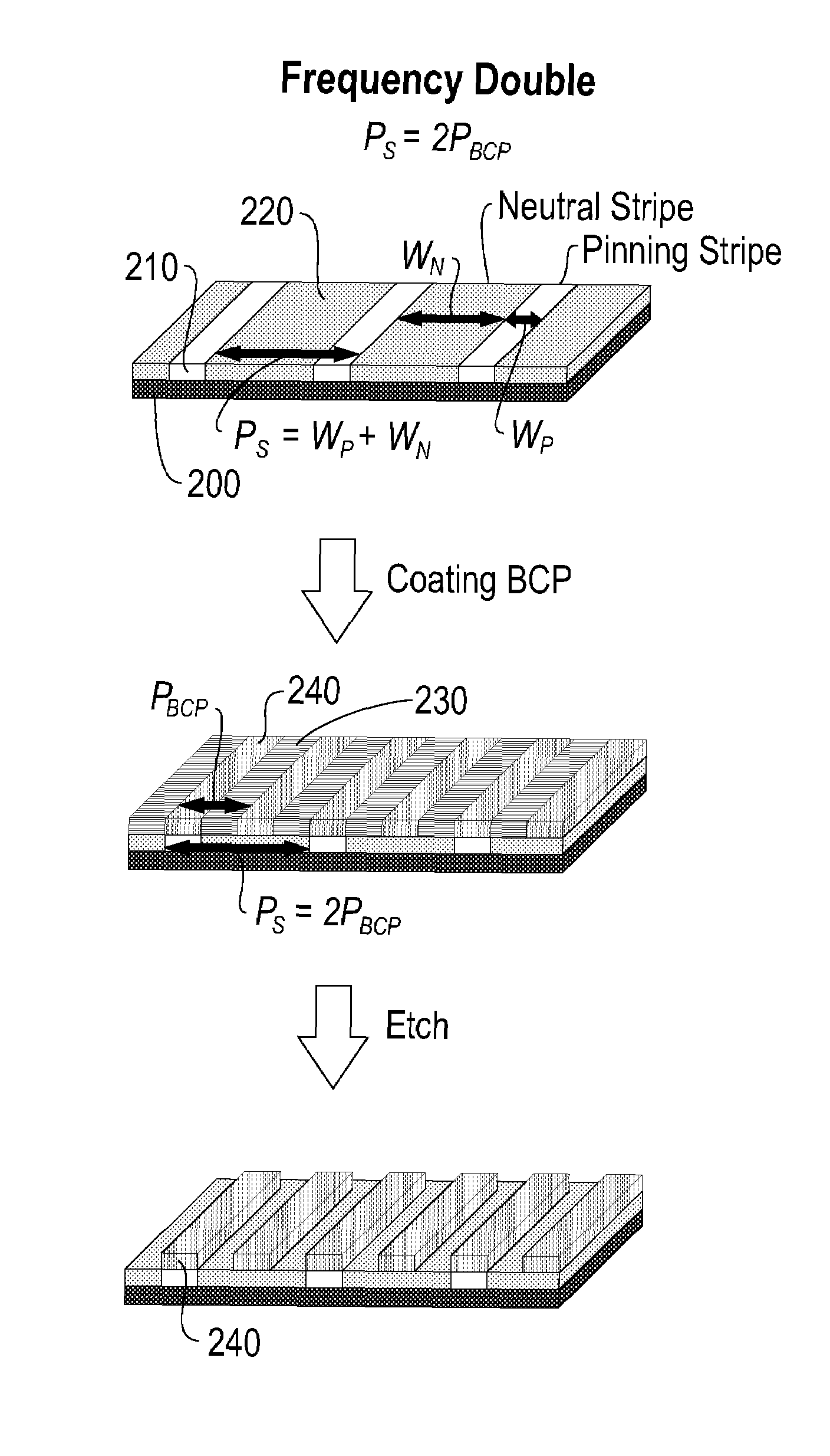
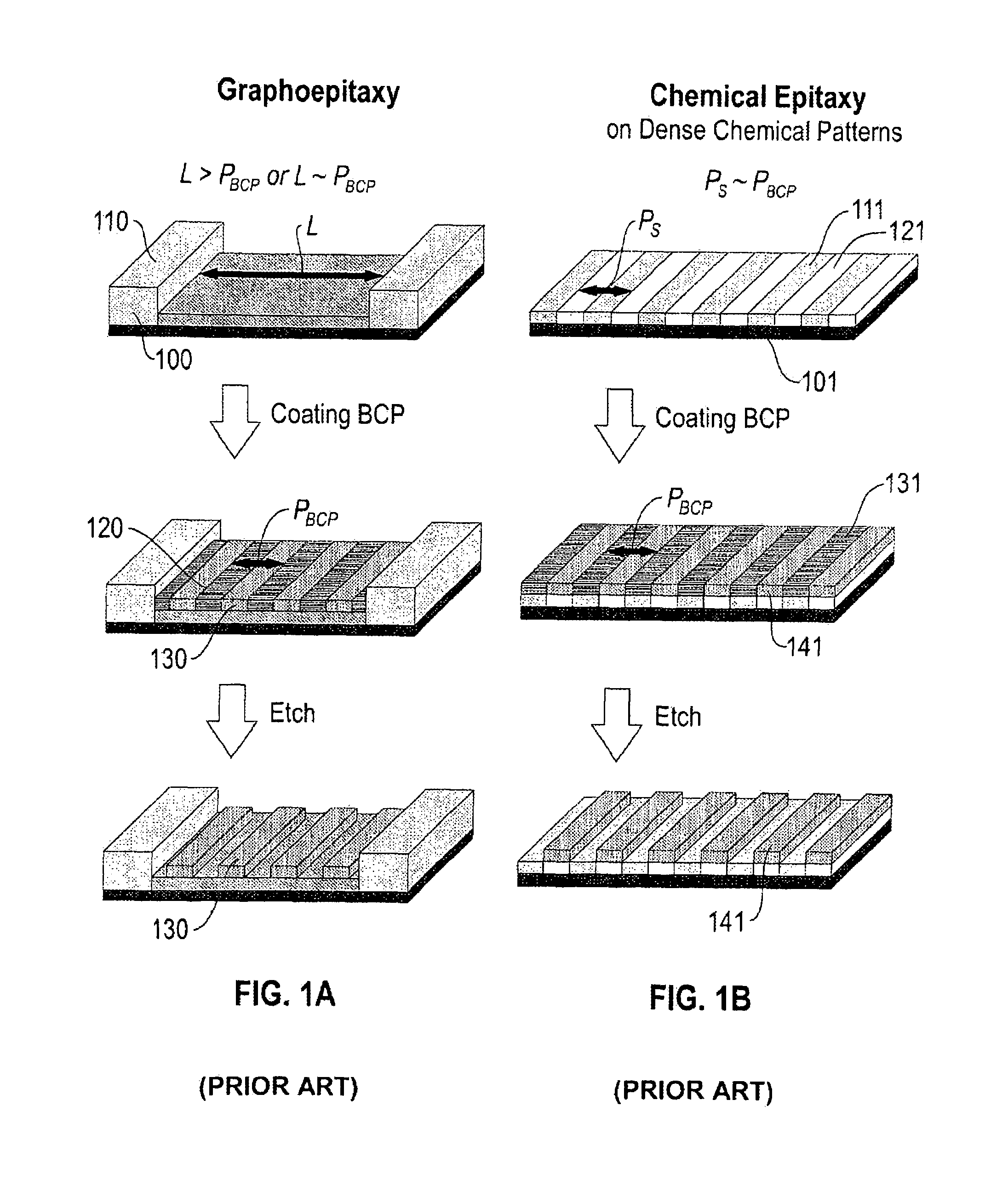
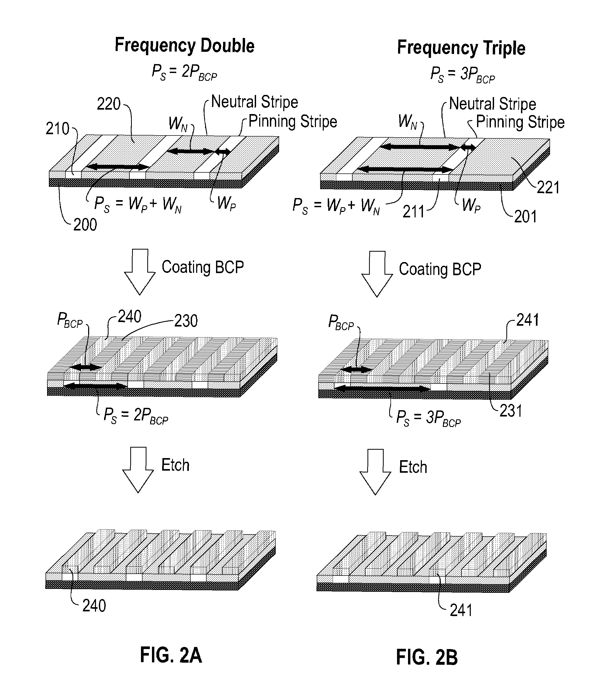
[0076]A sparse chemical pattern was prepared by a two-layer method in which a thin coating of hydridosilsesquioxane (HSQ) was cast on the top surface of cross-linked poly(epoxydicyclopentadienyl methacrylate epoxide-ran-styrene) (30:70 molar ratio, respectively; also abbreviated as PEpoxyDCPMA30-r-PS70), on a silicon substrate. The PEpoxyDCPMA30-r-PS70 layer was crosslinked using N-hydroxyphthalimide triflate as a thermal acid generator (10 wt % based on the total weight of thermal acid generator and polymer) by baking at 130° C. for 1 minute and then at 200° C. for 2 minutes. The PEpoxyDCPMA30-r-PS70 provided a neutral surface for poly(styrene-b-methylmethacrylate) (abbreviated as “PS-b-PMMA”), and HSQ provided a preferentially wettable surface for PMMA. The HSQ layer was imaged by direct write electron beam lithography and developed using an 0.26N tetramethylammonium hydroxide (TMAH) developer to generate a pattern of thin stripes having a total pitch of 57.5 nm, HSQ line...

Example

EXAMPLE 2

[0077]A sparse chemical pattern was made by a two-layer process as described in Example 1, with the chemical pattern prepared from a thin coating of hydridosilsesquioxane (HSQ) formed on thermally cross-linked PEpoxyDCPMA30-r-PS70. The HSQ layer was imaged and developed as in Example 1 to generate thin stripes with a pitch of 87.5 nm, an HSQ line width of 20 nm and an HSQ line height of 2.5 nm (FIG. 4A). A 1.5 wt % solution of PS-b-PMMA in PGMEA was then cast on the sparse chemical patterns of HSQ / PEpoxyDCPMA-r-PS and baked at 240° C. for 1 minute. The polymer domains in the PS-b-PMMA film self-aligned on top of the sparse chemical pattern to form a frequency tripled pattern of alternating PS and PMMA stripes with pitch of about 28.2 nm (FIG. 4B).

Example

EXAMPLE 3

[0078]A sparse chemical pattern was prepared by a two-layer method in which thin chromium (Cr) stripes were formed on the top surface of a thermally cross-linked organosilicate (OS) underlayer. The OS is a copolymer of methyltrimethoxysilane and tetraethoxysilane with a molecular weight Mw of 2,000 g / mol. The OS underlayer provides a neutral surface for the assembly of domains of the poly(styrene-b-ethylene oxide) (abbreviated PS-b-PEO, obtained from Polymer Source, with a molecular weight Mw for the PS block of 19,000 g / mol and for the PEO of 12,300 g / mol) cast along with a co-assembling OS component. The Cr surface serves as a preferentially wetted area for the PEO / OS domains. The sparse chemical pattern of thin Cr stripes having a pitch of 132 nm, a Cr linewidth of 20 nm, and a Cr line thickness of 2.5 nm was made by Cr deposition and liftoff of Cr from electron-beam patterned PMMA on the top surface of the OS underlayer. A 1% wt solution of PS-b-PEO and OS component (PS...


PUM

PropertyMeasurementUnit
Frequencyaaaaaaaaaa
Affinityaaaaaaaaaa

Abstract

Disclosed herein is a method of forming polymer structures comprising applying a solution of a diblock copolymer assembly comprising at least one diblock copolymer that forms lamellae, to a neutral surface of a substrate having a chemical pattern thereon, the chemical pattern comprising alternating pinning and neutral regions that are chemically distinct and which have a chemical pattern spatial frequency given by the number of paired sets of pinning and neutral regions along a given direction on the substrate; and forming domains comprising blocks of the diblock copolymer. The domains form by lateral segregation of the blocks. At least one domain has an affinity for the pinning regions and forms on the pinning region, the domains so formed on the pinning region are aligned with the underlying chemical pattern, and domains that do not form on the pinning region form adjacent to and are aligned with the domains formed on the pinning regions. In this way, a structure comprising repeating sets of domains is formed on the chemical pattern with a spatial frequency given by the number of repeating sets of domains in the given direction, that is at least twice that of the chemical pattern spatial frequency. Methods of forming the chemical patterns, and pattern transfer methods using patterned domains, are also disclosed.

Description

TRADEMARKS[0001]IBM® is a registered trademark of International Business Machines Corporation, Armonk, N.Y., U.S.A. Other names used herein may be registered trademarks, trademarks or product names of International Business Machines Corporation or other companies.BACKGROUND OF THE INVENTION[0002]1. Field of the Invention[0003]The invention relates to methods for aligning microdomains of block copolymers to chemical patterns that have a lower spatial frequency than the microdomains.[0004]2. Description of Background[0005]Patterns of ever smaller features having nanoscale critical dimensions (CD) allow denser circuitry to be created, thereby reducing overall production cost for electronic devices. Similarly, ever tighter pitches (i.e., feature spacing in a pattern) and smaller CDs are needed at each new technology node. Methods such as directed self-assembly of block copolymers (BCPs), in which the pitch of a pre-pattern defined by a lithography tool is subdivided, have been considere...

Claims


Application Information

Patent Timeline
IPC IPC(8): B05D3/00
CPCB82Y10/00B82Y40/00G03F7/0002
Inventor CHENG, JOYHINSBERG, WILLIAM D.KIM, HO-CHEOLRETTNER, CHARLES T.SANDERS, DANIEL P.
Owner GLOBALFOUNDRIES US INC
Why Eureka
Try Eureka