Light-sensing device

a light-sensing device and optical conversion technology, applied in the field of optical to electronic conversion, can solve the problems of increased noise, decreased light-detection performance, and weaker visible light signal than uv light signal,

Active Publication Date: 2009-04-21
QUANTUM SEMICON
View PDF3 Cites 120 Cited by
  • Summary
  • Abstract
  • Description
  • Claims
  • Application Information

AI Technical Summary

Benefits of technology

[0025]Another object of the invention is to provide a method of fabricating light-sensing devices including PIN and HIP photo-diode devices integrated with CMOS devices on a common semiconductor substrate and allowing the operational features of the devices to be tailored to suit various wavelength sensing requirements.
[0026]Yet another object of the invention is to provide a method of fabricating photo-detector devices including PIN and HIP photo-diode devices integrated with CMOS devices on a common semiconductor substrate and allowing the photo-diodes to be operated under Avalanche and Geiger modes.

Problems solved by technology

Therefore, solar-blind UV detection is achieved by reducing the thickness of the light sensing material, so that the signal generated by visible light is much weaker that the signal generated by UV light.
All these result increased noise and decreased performance of the light-detection, which can be counter-acted by further decreasing the operating temperature.
It has been very challenging to fabricate monolithically integrated sensors for the different wavelength bands (multi-spectral sensors), having pixel density and cost of fabrication comparable with the state of the art commercial CCDs and CMOS image sensors.
The main reason for this situation is the lack of suitable device / materials and process architectures capable of fabricating sensors covering most of the spectral ranges mentioned above.
For LWIR SiGe / Si HIP devices have also been fabricated but their performance seems considerably lower than that of MCT-based devices.
The fact that each range of wavelength requires a different type of photo-detector and / or a different materials system, has made impossible the fabrication of 1D and / or 2D arrays (or focal planes) of “color” pixels capable of capturing multiple-wavelengths in the visible and invisible parts of the spectrum, such as UV, Visible, SWIR, MWIR, LWIR.

Method used


Image

  • Light-sensing device
  • Light-sensing device
  • Light-sensing device

Examples


Embodiment Construction

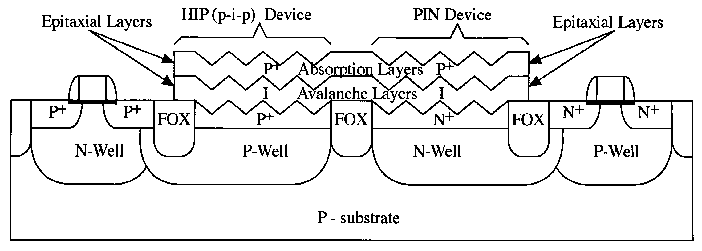
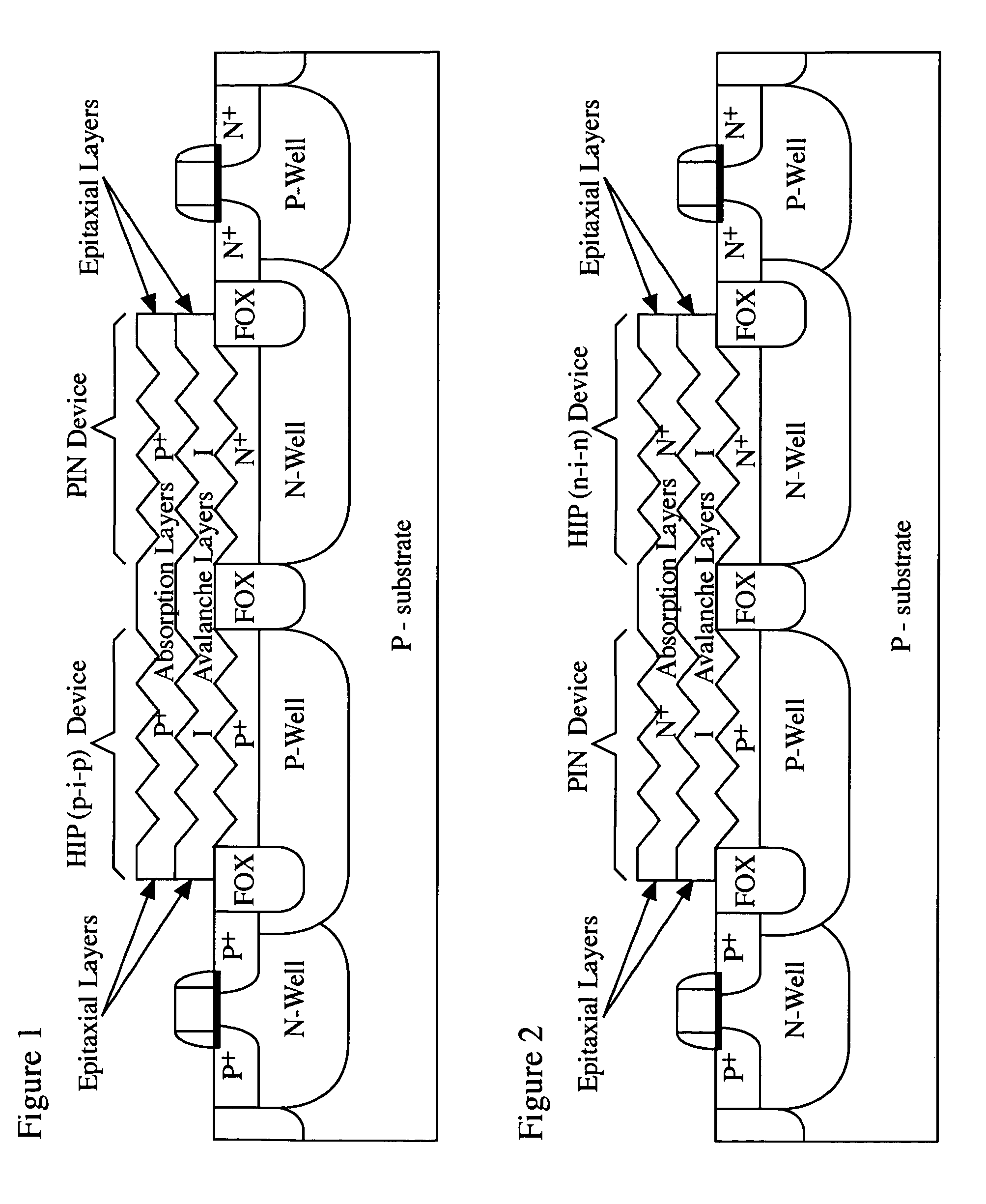
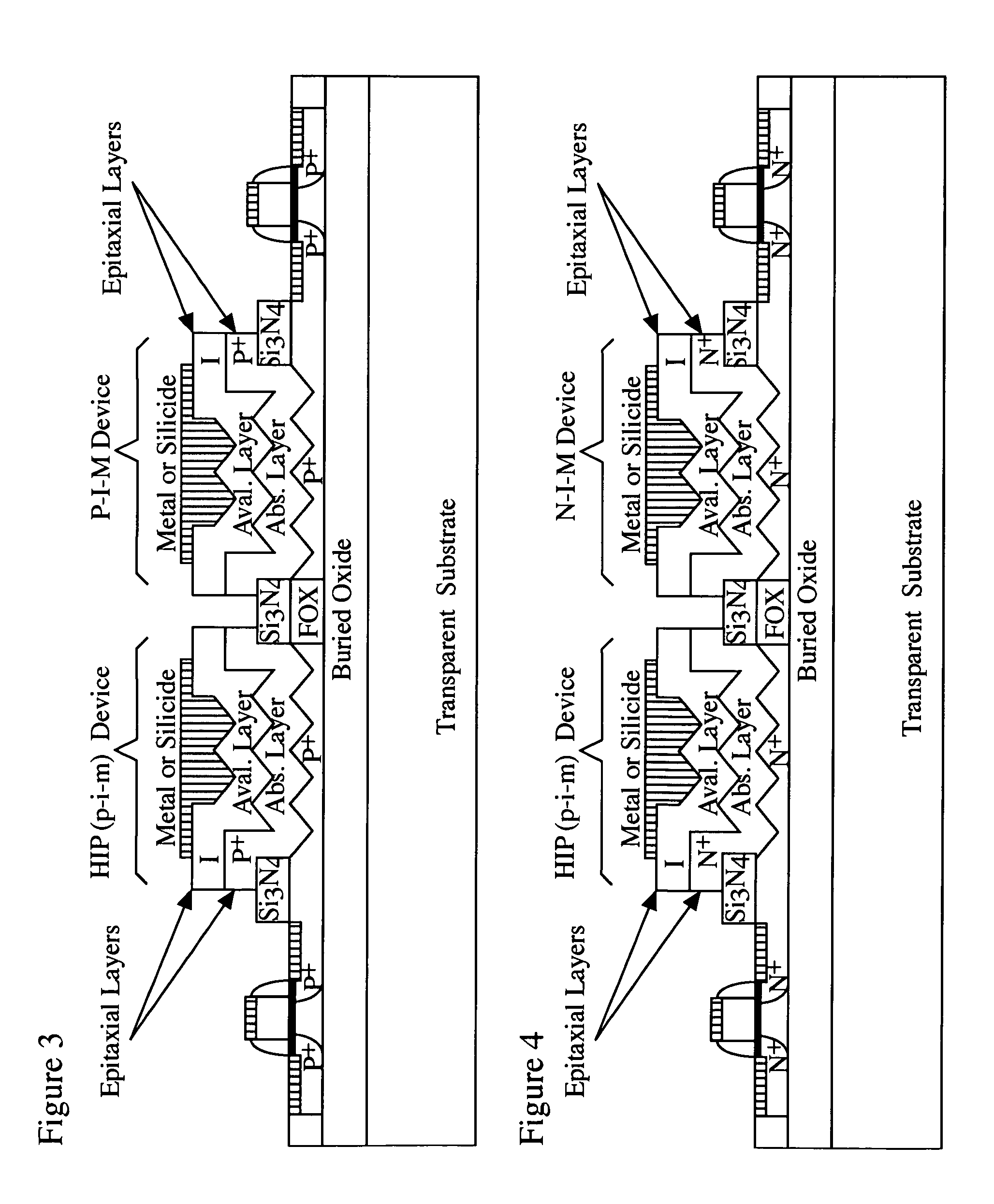
[0052]The present invention uses a process architecture which enables the fabrication of bandgap and doping engineered photodiodes, monolithically integrated with state of the art CMOS transistors. The exemplary process flow uses a selective or non-selective epitaxial growth of the photo-diode device layers on silicon-based or germanium-based substrates.

[0053]Epitaxial growth of PIN photo-diode devices integrated with CMOS devices on a semiconductor substrate is disclosed in WO / EP01 / 11817. One of the many advantages of fabricating PIN (or PN) photodiodes through the epitaxial growth process step on active area “windows” formed on the CMOS wafer, is the straightforward incorporation of Si1-x-yGexCy alloys and / or superlattices during the epitaxial growth thereby allowing the improvement of different device parameters, such as coefficient of absorption and bandgap engineering, with respect to similar devices made with pure silicon. Such possibility is not available to pn-junctions form...


PUM


Abstract

A method of fabricating light-sensing devices including photodiodes monolithically integrated with CMOS devices. Several types of photodiode devices (PIN, HIP) are expitaxially grown in one single step on active areas implanted in a common semiconductor substrate, the active areas having defined polarities. The expitaxially grown layers for the photodiode devices may be either undoped or in-situ doped with profiles suitable for their respective operation. With appropriate choice of substrate materials, device layers and heterojunction engineering and process architecture, it is possible to fabricate silicon-based and germanium-based multi-spectral sensors that can deliver pixel density and cost of fabrication comparable to the state of the art CCDs and CMOS image sensors. The method can be implemented with epitaxially deposited films on the following substrates: Silicon Bulk, Thick-Film and Thin-Film Silicon-On-Insulator (SOI), Germanium Bulk, Thick-Film and Thin-Film Geranium-On-Insulator (GeOI).

Description

CROSS REFERENCE TO RELATED APPLICATIONS[0001]This application is a Continuation application of PCT / EP2003 / 010346 filed Sep. 15, 2003, claiming priority of U.S. Patent Application No. 60 / 412,139 filed Sep. 19, 2002, which are included in their entirety by reference made hereto.BACKGROUND OF THE INVENTION[0002]The present invention relates to methods of optical to electronic conversion, in particular to photo-detection with devices suitable for integration with Complementary Metal Oxide Semiconductor (CMOS) technology.[0003]The devices and fabrication technologies used for light-sensing are highly dependent on the frequency or wavelength of the light to be sensed. Usually, for imaging purposes, the spectrum is divided into:[0004]Ultra-Violet (UV), wavelengths shorter than 0.4 μm[0005]Visible, wavelengths in the range of 0.4 μm to 0.7 μm[0006]Short-Wave Infra-Red (SWIR), wavelengths in the range of 1 μm to 3 μm[0007]Mid-Wave Infra-Red (MWIR), wavelengths in the range of 3 μm to 5 μm[00...

Claims


Application Information

Patent Timeline
Patent Type & Authority Patents(United States)
IPC IPC(8): H01L21/00H01L27/02H01L27/144H01L27/146H01L31/00H01L31/0232H01L31/0328H01L31/10H01L31/107
CPCH01L27/14643H01L27/14669H01L27/14609H01L27/14625H01L27/14665H01L31/0232H01L31/107H01L31/1075
Inventor AUGUSTO, CARLOS J. R. P.
Owner QUANTUM SEMICON
Why Eureka
Try Eureka