Semiconductor device and method of manufacturing the same

a semiconductor and manufacturing method technology, applied in the manufacture of printed circuits, printed circuit aspects, basic electric elements, etc., can solve the problems of chip and wiring substrate not being fully filled, under-filling may not be good, and the wiring substrate was not fully filled, so as to prevent the generation of twisting and distortion of the wiring substrate, the effect of high precision

Active Publication Date: 2009-04-21
RENESAS ELECTRONICS CORP
View PDF22 Cites 17 Cited by
  • Summary
  • Abstract
  • Description
  • Claims
  • Application Information

AI Technical Summary

Benefits of technology

[0010]The present invention was made in order to solve the above problems. The first purpose is to obtain a semiconductor device which can prevent the generation of twist and distortion of a wiring substrate, even when the stiffener is omitted.
[0023]By the method of manufacturing a semiconductor device according to the sixth aspect of the present invention, even when the shape is made to have a clearance between the portion which projects to the perimeter of the chip of the heat spreader, and the wiring substrate upper surface, a heat spreader's hitting a formation instrument and a test instrument, and damaging can be prevented in the case of formation of a solder ball.

Problems solved by technology

Hereby, there were problems that the solder ball joined to the under surface of the wiring substrate floated, or a stress was applied to the edge of the semiconductor chip.
There was a problem that the adhesion of a semiconductor chip, a wiring substrate, and under-filling may not be good, and the gap of the semiconductor chip and the wiring substrate was not fully filled up with under-filling resin.
And in an argon spatter, argon etc. could not fully be supplied to the narrow gap of the semiconductor chip and the wiring substrate, and the adhesion of the gap concerned has not fully been improved.
When the stiffener is omitted for cost reduction, the shape is made to have a clearance between the portion which projects to the perimeter of the chip of the heat spreader, and the wiring substrate upper surface, and heat radiation resin is thin, a crack and a damage will enter into the semiconductor chip easily.
On the other hand, when heat radiation resin is thick, the divergence characteristics of heat will worsen.
In the case that the stiffener is omitted, and the shape is made to have a clearance between the portion which projects to the perimeter of the chip of the heat spreader, and the wiring substrate upper surface, when a solder ball is formed on the under surface of the wiring substrate, and doing an electric test of the wiring substrate and the semiconductor chip after that, there was also a problem of the heat spreader having hit a formation instrument and a test instrument, and damaging.

Method used


Image

  • Semiconductor device and method of manufacturing the same
  • Semiconductor device and method of manufacturing the same
  • Semiconductor device and method of manufacturing the same

Examples


embodiment 1

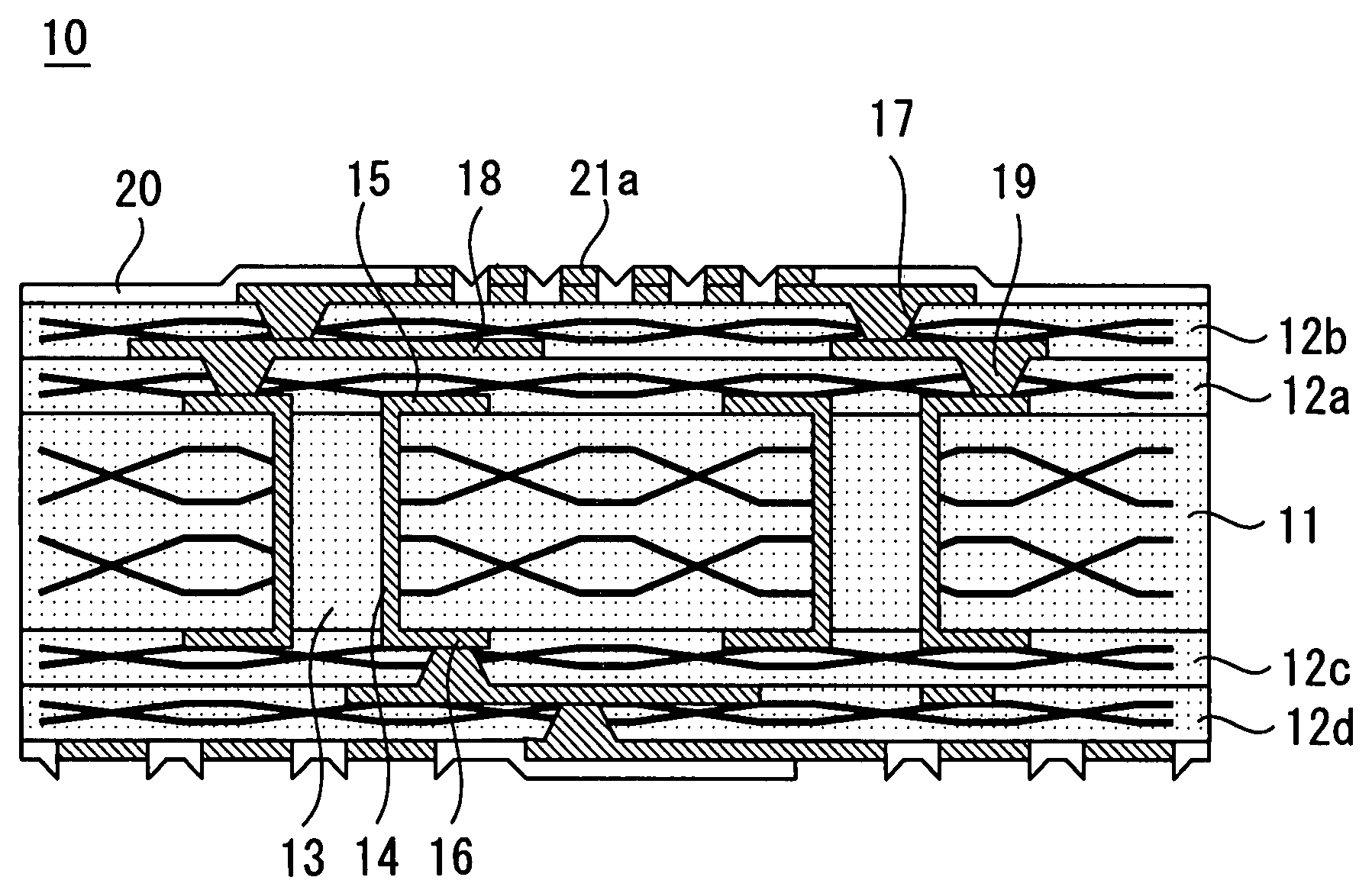
[0047]Hereafter, the manufacturing method of the semiconductor device concerning Embodiment 1 of the present invention is explained using drawings.

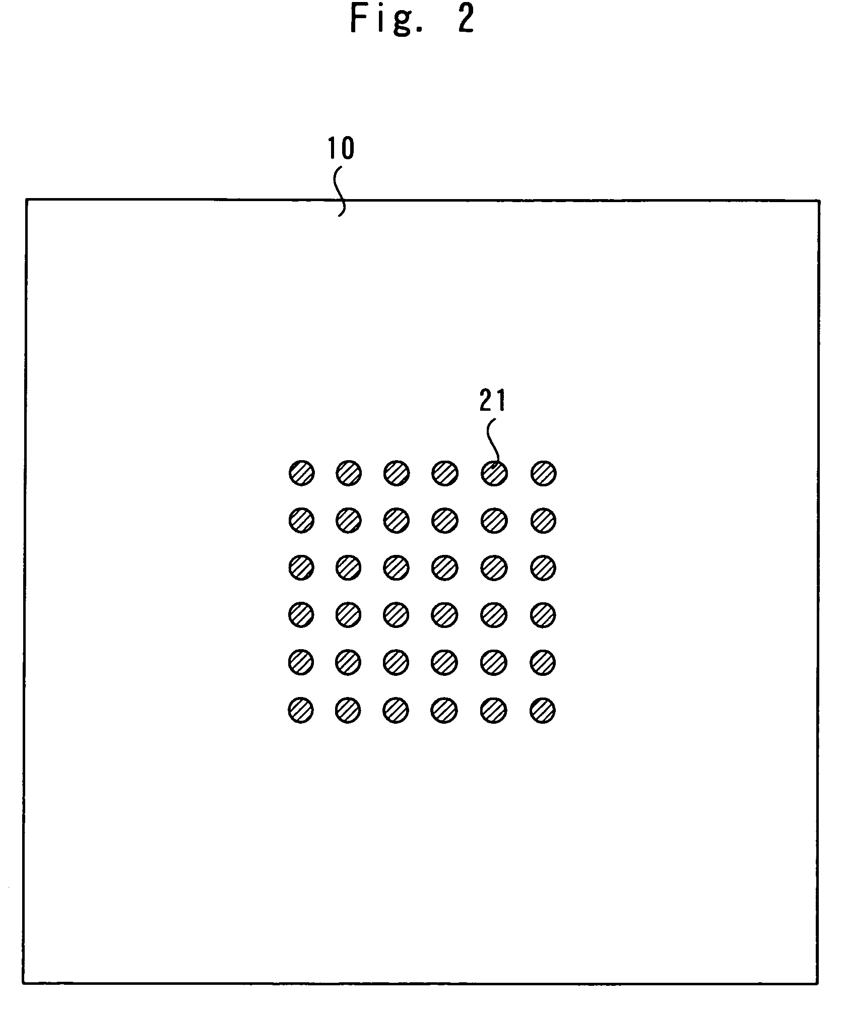
[0048]FIG. 1 is a sectional view showing the wiring substrate of the semiconductor device concerning Embodiment 1 of the present invention, FIG. 2 is the top view, and FIG. 3 is the bottom view.

[0049]This wiring substrate 10 puts build-up substrates 12a and 12b on the upper surface of core substrate 11, puts build-up substrates 12c and 12d on the under surface, and is made to unify by thermo-compression using a vacuum press etc. However, in order to prevent a warp of wiring substrate 10, the build-up substrate of the same number of sheets is bonded together to the upper and lower sides of core substrate 11.

[0050]And core substrate 11 and build-up substrates 12a-12d include a layer in which the glass cloth was impregnated with insulating resin to solidify into a plate, respectively. Here, the textile fabrics which include long glass textil...

embodiment 2

[0091]FIG. 22 is a sectional view showing the semiconductor device concerning Embodiment 2 of the present invention. The difference with Embodiment 1 is using the thing which made thin insulating substrates 43a-43d in which the through hole less than or equal to 100 μm was formed for the diameter bond by thermo-compression with a vacuum press etc., and made them unify, not using a core substrate as wiring substrate 10. However, each insulating substrates 43a-43d include the layer in which the glass cloth was impregnated with insulating resin, respectively, and was solidified platy. Other structure is the same as that of Embodiment 1.

[0092]Hereby, rigidity can be made high as the wiring substrate 10 whole. Therefore, even when the stiffener is omitted for cost reduction, a warp and a distortion of wiring substrate 10 can be prevented.

embodiment 3

[0093]In Embodiment 3, heat radiation property is improved using the thing smaller than Embodiment 1 as a filler mixed in heat radiation resin 31. Concretely, the filler whose average particle diameter is 5.8 μm and whose maximum grain size is 24 μm is used.

[0094]And in order to control the thickness of heat radiation resin 31, a spacer which includes globular form zirconia is mixed in heat radiation resin 31. Concretely, the spacer whose average particle diameter is 25 μm and whose maximum grain size is 33 μm is used. The thickness of heat radiation resin 31 is controllable by this spacer to 60±20 μm.

[0095]That is, the desired thickness of heat radiation resin is set to A, average particle diameter of a spacer is set to C, and a spacer is chosen so that it may have the relation:

A× 9 / 10≦C.

Hereby, the thickness of heat radiation resin is controllable within fixed limits centered on desired thickness.

[0096]And by setting the maximum grain size of a filler to BMAX, and the maximum gra...


PUM

PropertyMeasurementUnit
diameteraaaaaaaaaa
diameteraaaaaaaaaa
diameteraaaaaaaaaa

Abstract

Even when a stiffener is omitted, the semiconductor device which can prevent the generation of twist and distortion of a wiring substrate is obtained.As for a semiconductor device which has a wiring substrate, a semiconductor chip by which the flip chip bond was made to the wiring substrate, and a heat spreader adhered to the back surface of the semiconductor chip, and which omitted the stiffener for reinforcing a wiring substrate and maintaining the surface smoothness of a heat spreader, a wiring substrate has a plurality of insulating substrates in which a through hole whose diameter differs, respectively was formed, and each insulating substrate contains a glass cloth.

Description

CROSS-REFERENCE TO RELATED APPLICATIONS[0001]The present application claims priority from Japanese patent applications No. 2005-121063 filed on Apr. 19, 2005, and No. 2006-096999 filed on Mar. 31, 2006, the content of which is hereby incorporated by reference into this application.FIELD OF THE INVENTION[0002]The present invention relates to a semiconductor device which makes flip chip connection of a semiconductor chip on a wiring substrate, and forms a heat spreader on a back surface of this semiconductor chip, and its manufacturing method.DESCRIPTION OF THE BACKGROUND ART[0003]A semiconductor device which makes flip chip connection of the semiconductor chip via the bump on the wiring substrate is proposed. The gap of the semiconductor chip and the wiring substrate is filled up with under-filling resin in this semiconductor device. In order to make heat radiation property high, a heat spreader is formed on the back surface of the semiconductor chip. In order to reinforce a wiring s...

Claims


Application Information

Patent Timeline
Patent Type & Authority Patents(United States)
IPC IPC(8): H01L23/48H01L23/52H01L29/40
CPCH01L21/4853H01L21/563H01L21/6835H01L23/36H01L23/49822H01L23/49894H01L24/16H01L24/81H05K3/4602H01L24/29H01L24/32H01L23/562H01L24/743H01L23/49811H01L2224/11003H01L2224/13099H01L2224/16225H01L2224/73203H01L2224/73204H01L2224/73253H01L2224/81193H01L2224/81205H01L2224/81801H01L2224/83102H01L2224/92125H01L2924/01005H01L2924/01013H01L2924/01018H01L2924/01022H01L2924/01029H01L2924/0105H01L2924/01074H01L2924/01078H01L2924/01082H01L2924/12044H01L2924/13091H01L2924/15174H01L2924/15184H01L2924/15311H01L2924/15312H05K1/0366H05K2201/029H01L2924/01006H01L2924/01019H01L2924/01033H01L2924/014H01L2224/32225H01L2224/29111H01L2924/0133H01L2924/15724H01L2924/15747H01L2924/1579H01L2224/2919H01L2224/131H01L2924/1306H01L2924/0132H01L2924/01014H01L2924/00H01L2924/00012H01L2924/0665H01L2924/3512H01L2924/351H01L2924/12042H01L2224/05024H01L2224/05008H01L2224/05009H01L2224/05022H01L2224/05025H01L2224/05023H01L2224/05001H01L2224/05572H01L2224/05124H01L2224/056H01L2224/06131H01L2924/00014H01L24/11H01L2224/16227H01L2224/81909H01L2021/6015H01L23/3157H01L23/373H01L23/49816H01L23/49827H01L23/49838H01L23/3142
Inventor HAYASHI, EIJIGO, KYOHARADA, KOZOBABA, SHINJI
Owner RENESAS ELECTRONICS CORP
Why Eureka
Try Eureka