Method for correcting astigmatism in a microlithography projection exposure apparatus, a projection objective of such a projection exposure apparatus, and a fabrication method for micropatterned components

Inactive Publication Date: 2009-04-21
CARL ZEISS SMT GMBH
View PDF7 Cites 5 Cited by
  • Summary
  • Abstract
  • Description
  • Claims
  • Application Information

AI Technical Summary

Benefits of technology

[0020]It is an object of the present invention to provide a method with the aid of which it is possible to correct field-constant astigmatism with the least possible outlay in the case of a non-rotationally symmetrical projection objective.
[0021]It is further an object of the present invention to provide a not rotationally symmetrical projection objective that renders it possible to correct field-constant astigmatism.
[0022]It is a further object of the present invention to provide a method for the microlithographic fabrication of micropatterned components that is improved with regard to its accuracy of application.
[0024]The invention is based on the finding that linear astigmatism and field-constant astigmatism, in particular, are similar in an off-axis partial annular image field. According to the invention, by adjusting the position of at least one of the optical elements in the off-axis field region of the image field a linear and / or quadratic astigmatism are / is induced which is directed opposite to the field-constant astigmatism and can therefore at least partly compensate the latter. The correction of a field-constant astigmatism by means of adjusting the position of single optical elements or a number thereof has the advantage that there is no need for an actively deformable optics when the field-constant astigmatism changes with time during operation. The adjustment of the position of single optical elements or a number thereof constitutes a mechanism for correcting field-constant astigmatism that is simple even during operation of the projection objective.
[0028]It can preferably be provided for the purpose of further improving the correction of field-constant astigmatism to additionally produce a quadratic astigmatism by adjusting the position of at least one optical element and / or of the object in the off-axis field region.

Problems solved by technology

With the rising demands placed on the resolution of the microfeatures to be imaged, aberrations caused by the projection objective are increasingly posing a problem.
Thus, there is no image plane in which the two lines can simultaneously be sharply imaged and, in the case of a projection objective this leads to a loss of imaging accuracy because of the complexity of the features to be imaged.
The cause of astigmatism can lie, for example, in fabrication errors of the surfaces or of the material (for example an inhomogeneous refractive index for objectives with refractive elements) of the optical elements, in deformations of optical elements owing to external forces or torques that are caused by nonideal mounts or screw joints and their assembly, in non-uniform thermal expansions of near-pupil optical elements during operation (for example owing to radiation with light) and / or in a nonuniform degradation of the material of the optical elements during use of the projection objective.
Unlike the rotationally symmetrical projection objectives, because of the lack of rotational symmetry with such a projection objective the field-constant astigmatism cannot be corrected by clocking.
However, since the field-constant astigmatism can vary with time during operation of the projection objective, such a deformation requires an actively deformable optics, and this is associated with a substantial level of structural complexity, and thus with a high outlay on cost.
Since clocking does not generally constitute a solution to the correction of astigmatism in the case of not rotationally symmetrical projection objectives, the only possibility left would be to provide an actively deformable optics in general, with the disadvantage of the very high technical requirements with reference to accuracy of setting, operational stability and high costs.

Method used


Image

  • Method for correcting astigmatism in a microlithography projection exposure apparatus, a projection objective of such a projection exposure apparatus, and a fabrication method for micropatterned components
  • Method for correcting astigmatism in a microlithography projection exposure apparatus, a projection objective of such a projection exposure apparatus, and a fabrication method for micropatterned components
  • Method for correcting astigmatism in a microlithography projection exposure apparatus, a projection objective of such a projection exposure apparatus, and a fabrication method for micropatterned components

Examples


Embodiment Construction

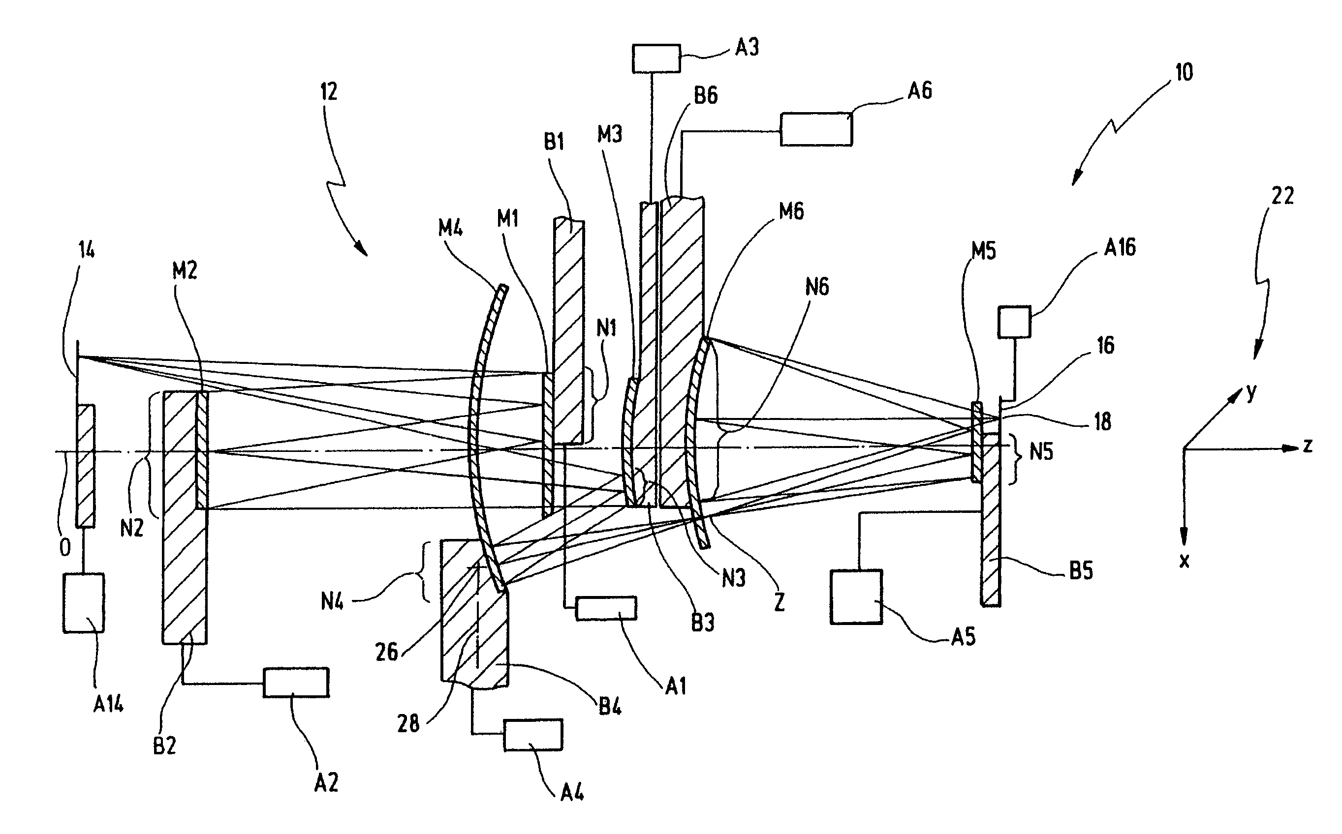
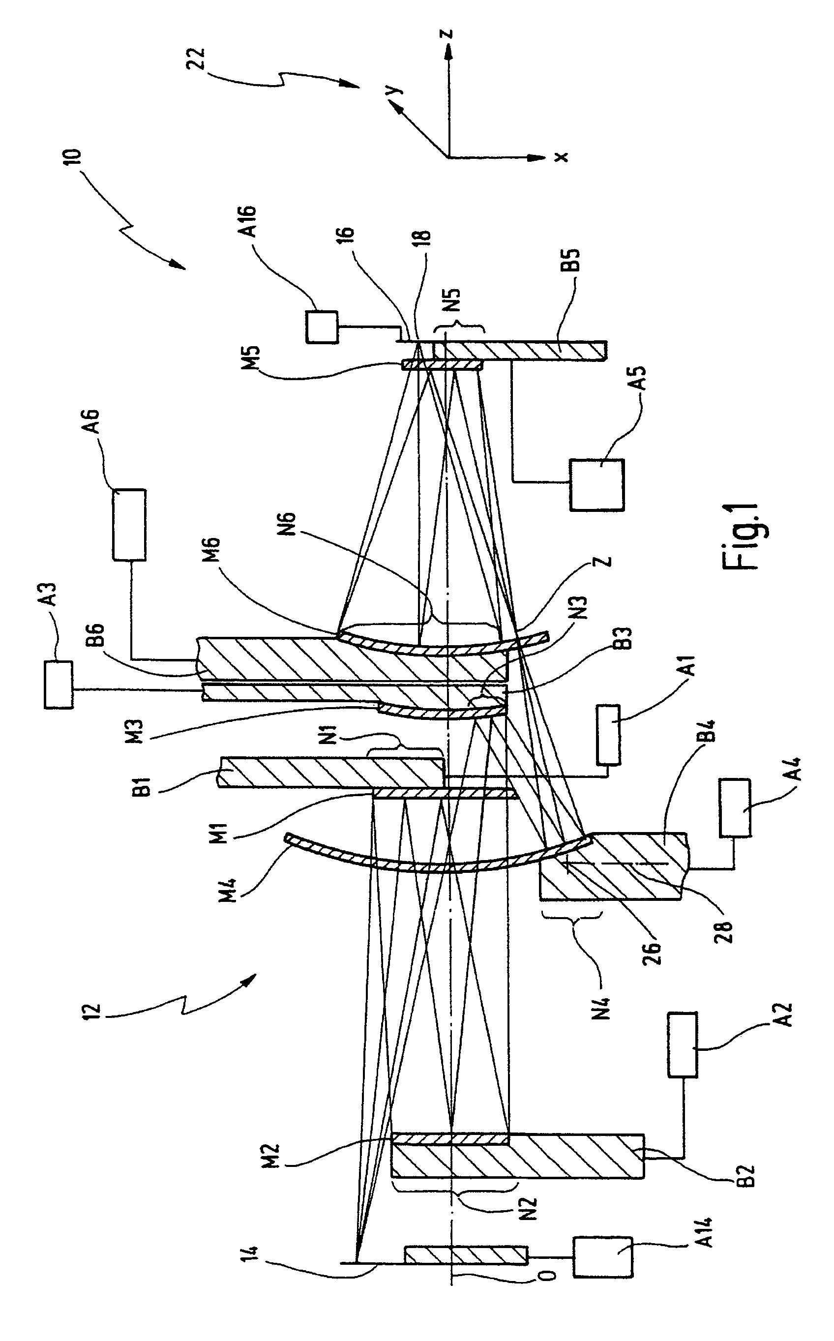
[0049]A microlithography projection exposure apparatus provided with the general reference numeral 10 is illustrated in FIG. 1 in the region of a projection objective 12. Further components of the projection exposure apparatus 12 such as, for example, the light source or the illumination system between the light source and the projection objective 10 are not illustrated.

[0050]The projection exposure apparatus 10 preferably operates in the EUV spectral region at a wavelength of 13 nm.

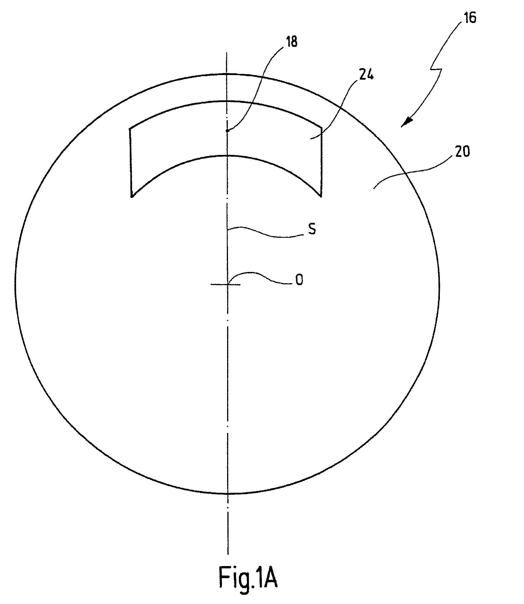
[0051]A pattern (not illustrated in more detail) of an object 14 that is arranged in an object plane and denoted in microlithography as a reticle is imaged by means of the projection objective 12 onto a substrate 16 that is coated with a light-sensitive material and is also denoted as a wafer in microlithography. The substrate 16 is located in the image plane of the projection objective 12.

[0052]The projection objective 12 has a plurality of optical elements in the form of mirrors M1, M2, M3, M4, M5, M6....


PUM


Abstract

A method for correcting a field-constant astigmatism of a projection objective of a microlithography projection exposure apparatus, the projection objective having an arrangement composed of a plurality of optical elements that images at least a part of an object onto an off-axis image field lying outside at least one optical axis, the arrangement of the plurality of optical elements having a plane of symmetry that is defined by the at least one optical axis and a center of the image field, includes adjusting a position of at least one element of the plurality of optical elements in such a way that at least one linear and / or quadratic astigmatism is produced that compensates the field-constant astigmatism at least partially. A projection objective of a projection exposure apparatus, as well as a microlithographic method for producing micropatterned components uses the method.

Description

PRIOR APPLICATION[0001]The present application claims priority of U.S. Provisional Application No. 60 / 614,184 filed on Sep. 29, 2004.BACKGROUND OF THE INVENTION[0002]The invention relates in general to the field of microlithography.[0003]The invention relates in this field to a method for correcting a field-constant astigmatism of a projection objective of a microlithography projection exposure apparatus.[0004]The invention also relates to a projection objective of a microlithography projection exposure apparatus.[0005]The invention also relates to a method for the microlithographic production of micropatterned components and to a micropatterned component produced in such a way.[0006]Micropatterned components, for example highly integrated electric circuits, are produced microlithographically in the semiconductor industry.[0007]For this purpose, at least one layer made from a light-sensitive material, for example a photoresist, is applied to a substrate, for example a silicon wafer....

Claims


Application Information

Patent Timeline
IPC IPC(8): G03B27/68G02B5/10
CPCG02B17/0657G03F7/70233G03F7/706
Inventor KIRCHNER, ANDREASMANN, HANS-JUERGENKNEER, BERNHARD
Owner CARL ZEISS SMT GMBH
Why Eureka
Try Eureka