Solid-state lateral emitting optical system

a lateral emitting optical system and solid-state technology, applied in the direction of instruments, lighting and heating apparatus, semiconductor devices for light sources, etc., can solve the problems of failure of the total internal reflection (tir) principle, undesired redirection of light outside the desired angle for both tir and reflective coating designs, and the failure of the total internal reflection principl

Inactive Publication Date: 2009-04-28
DICON FIBEROPTICS +1
View PDF8 Cites 55 Cited by
  • Summary
  • Abstract
  • Description
  • Claims
  • Application Information

AI Technical Summary

Problems solved by technology

However some issues remain.
Any variation of the position of the chip leads to a failure of the Total Internal Reflection (TIR) principle and undesired redirection of light outside of the desired angle for both TIR and reflective-coating designs.
Moreover single chip devices present several limitations for backlighting applications.
Each of these elements reduces the overall light transmission of the system.
This would be a barrier for any LCD application.
The size, the weight and the cost of the lens would be far beyond the requirements of LCD TV and projectors.

Method used


Image

  • Solid-state lateral emitting optical system
  • Solid-state lateral emitting optical system
  • Solid-state lateral emitting optical system

Examples


Embodiment Construction

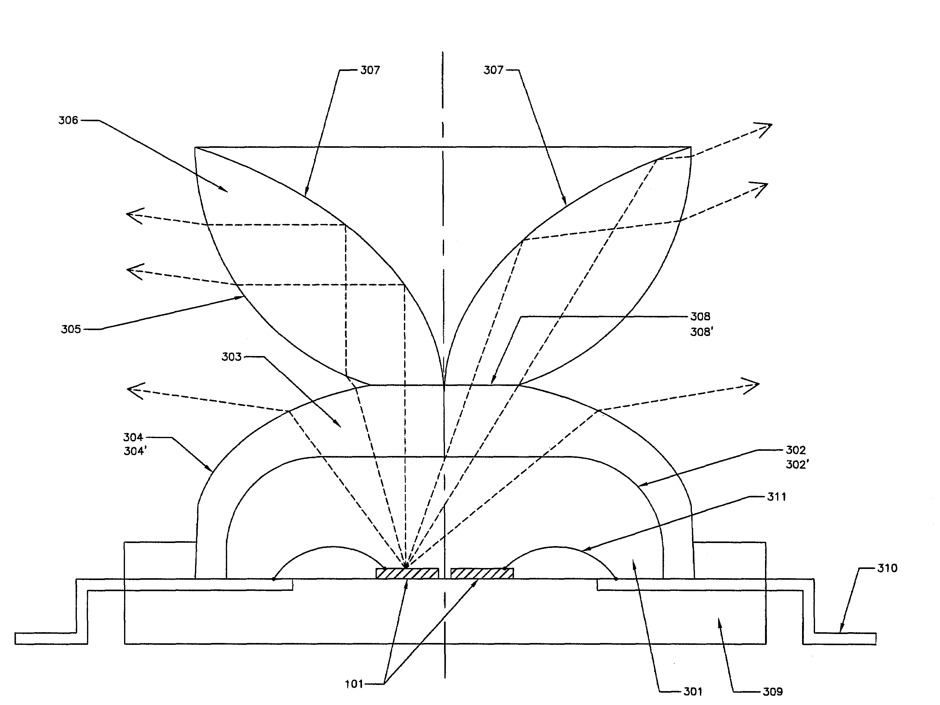
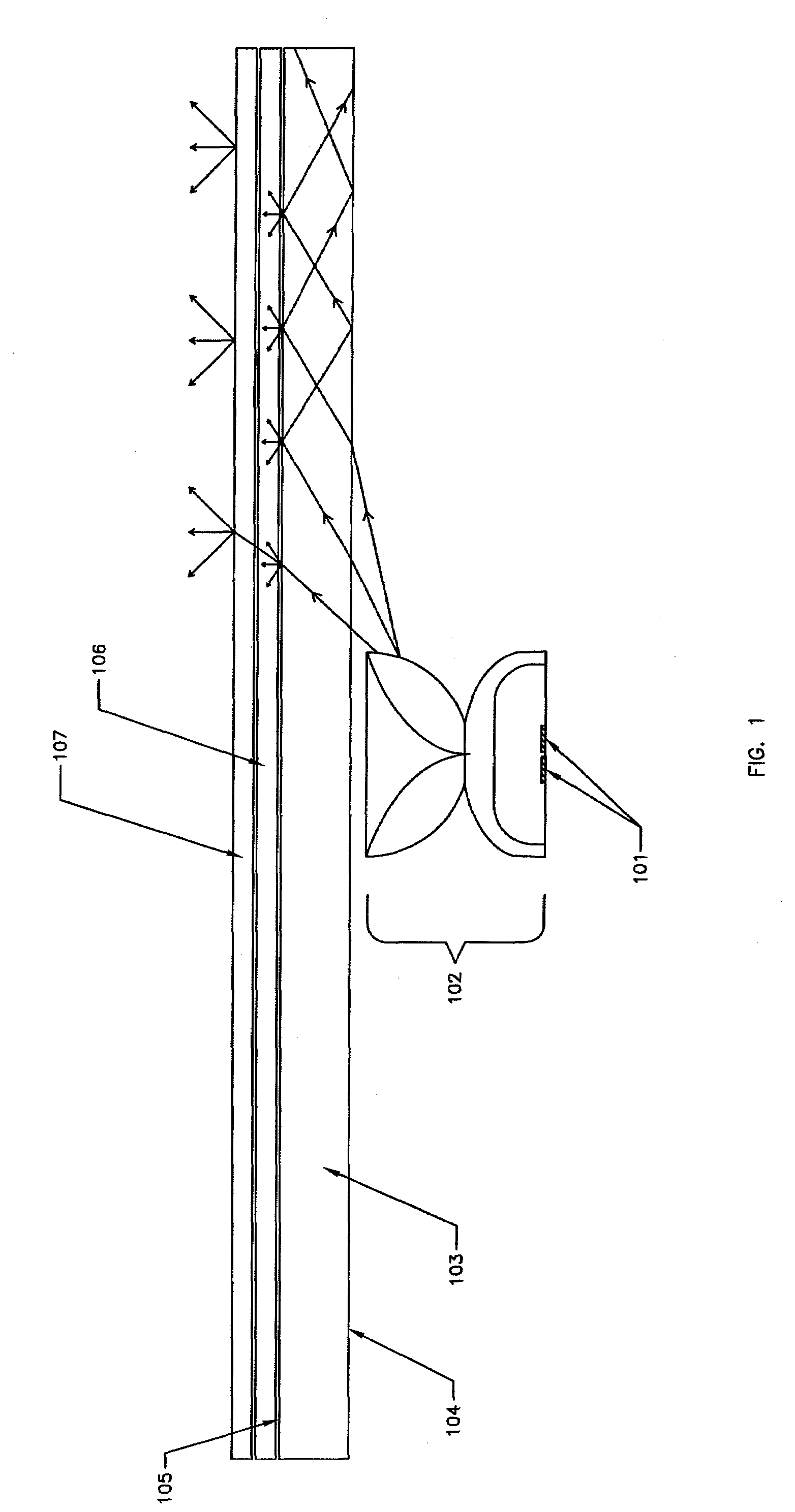
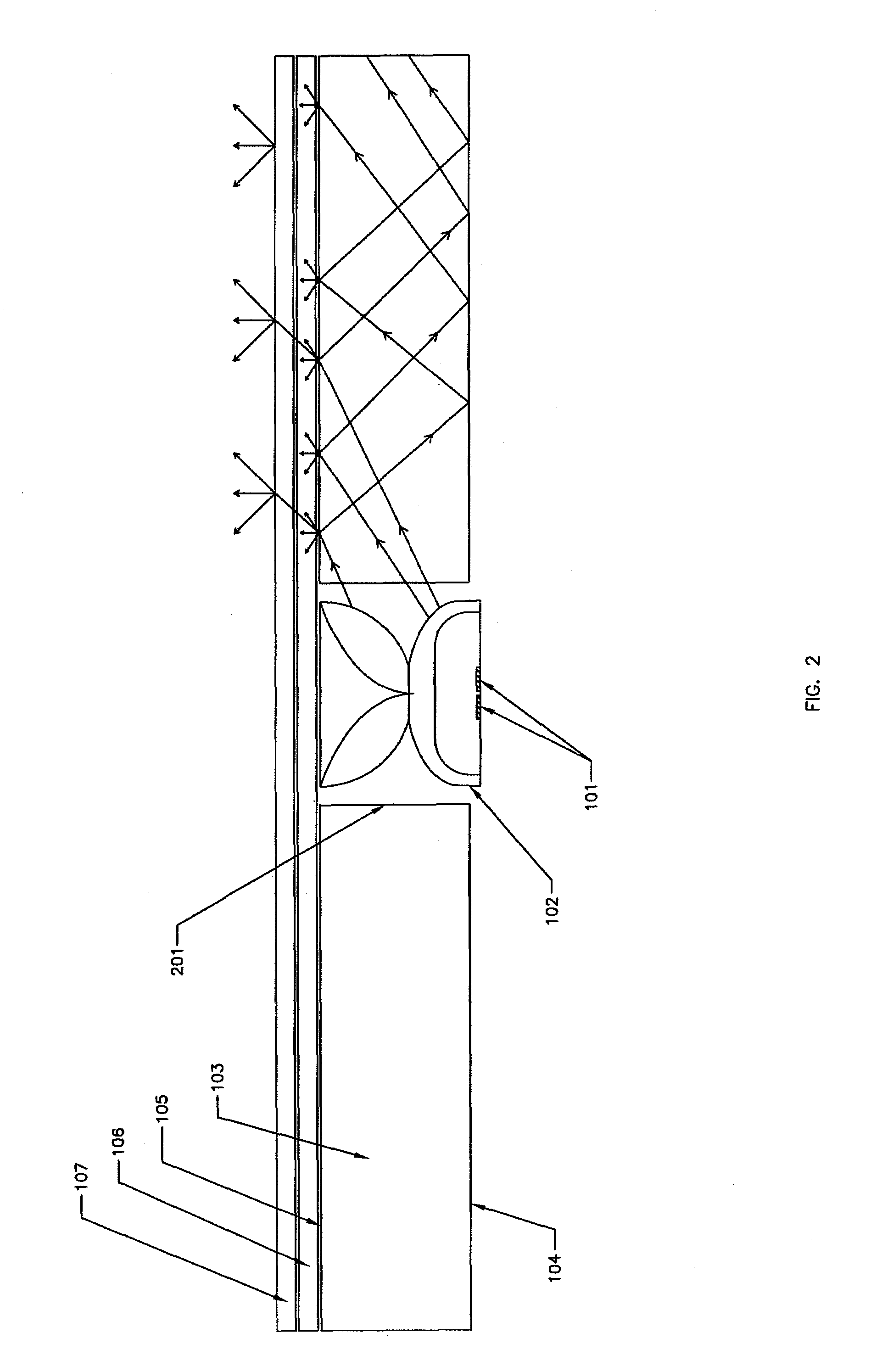
[0027]Integrating multiple LED chips with same or different colors in a compact compartment, as a lateral emitting cell is desirable for better color control, color mixing and lower cost. But it is very difficult to manage light output from multiple light chips with a single lens. Previous art provides solutions for a light cell with a single chip. However to the best of our knowledge, none of them describes an efficient solution based on a single lens for multiple chips.

[0028]The embodiments of this present invention provide a lens that will accommodate at least 2 light emitting chips and couple about 90% of the light emitted by these chips into a lightguide. The embodiments achieve such a high coupling efficiency while keeping the lateral and vertical dimensions of the lens preferably less than five times the lateral dimension of the light emitting area.

[0029]In one embodiment of the invention, the reflective surface is uncoated and the reflection is caused by total internal refle...


PUM


Abstract

The optical lens embodiment of the invention refracts and reflects light emitted from the light emitting diode chips on a unique combination of curved surfaces to obtain the desired coupling to a lateral light guide. The system of curved surfaces redirects rays from multiple LED chips laterally by multiple refraction and / or reflection. The optical lens has an optical axis, and comprises a bottom surface and a curved reflecting surface having a concave side. The concave side is oriented to face said bottom surface at an oblique angle. The reflecting surface surrounds the optical axis. The lens comprises a first curved refracting surface having a concave side facing the concave side of the reflecting surface and a second refracting surface extending as a smooth curve from the bottom surface to the first refracting surface. Light entering the lens through the bottom surface and directly incident on the reflecting surface is reflected from the reflecting surface at its concave side to the first refracting surface and refracted by the first refracting surface to exit the lens in a lateral direction with respect to the optical axis of the lens. A first portion of light entering the lens through the bottom surface and directly incident on the second refracting surface is refracted by the second refracting surface to exit the lens in a lateral direction with respect to the optical axis of the lens. A second portion of light entering the lens through the bottom surface and directly incident on the second refracting surface is refracted by the second refracting surface to the first refracting surface, refracted by the first refracting surface to the reflecting surface, reflected by the reflecting surface at its concave side to the first refracting surface and refracted by the first refracting surface to exit the lens in a lateral direction with respect to the optical axis of the lens.

Description

BACKGROUND OF THE INVENTION[0001]Recent progresses in the field of Light Emitting Diodes (LEDs) have opened the field to new families of applications.[0002]Improvements of internal quantum efficiency and improvement of the extraction efficiency strategies have led to LED chips that deliver high flux. By using high performance packages, LED-based devices at higher driving currents have been developed. Consequently, performance and reliability of LED-based devices have reached new standards, opening ways for high brightness, color-sensitive applications. With this level of performance, LEDs have become a viable alternative to Cold Cathode Fluorescent Lamp (CCFL) for LCD backlighting.[0003]Compared to CCFL, LEDs offer a new level of flexibility to LCD designers. New generations of LEDs promise to reshape and eventually reduce power consumption. They also offer the possibility of an independent control of various combinations to produce the desired lighting effect.[0004]For example, the...

Claims


Application Information

Patent Timeline
Patent Type & Authority Patents(United States)
IPC IPC(8): F21V8/00
CPCG02B19/0066G02B19/0071G02B19/0028F21V5/04F21V5/046F21V7/0091F21Y2101/02H01L25/0753H01L33/58H01L2924/0002H01L2924/00F21Y2115/10
Inventor VENNETIER, PERIGNAULIN, JEAN-YVES
Owner DICON FIBEROPTICS
Why Eureka
Try Eureka