

Active matrix display devices and the manufacture thereof
a technology of active matrix and display device, which is applied in the direction of identification means, instruments, optics, etc., can solve the problems of affecting the use of tfts manufactured using mic techniques, unsuitable for use in applications such as the pixel area of amlcds, etc., and achieves the reduction of the time taken by this step, the simplified manufacturing process, and the effect of reducing the time taken
- Summary
- Abstract
- Description
- Claims
- Application Information
AI Technical Summary
Benefits of technology
Problems solved by technology
Method used
Image

Examples
Embodiment Construction
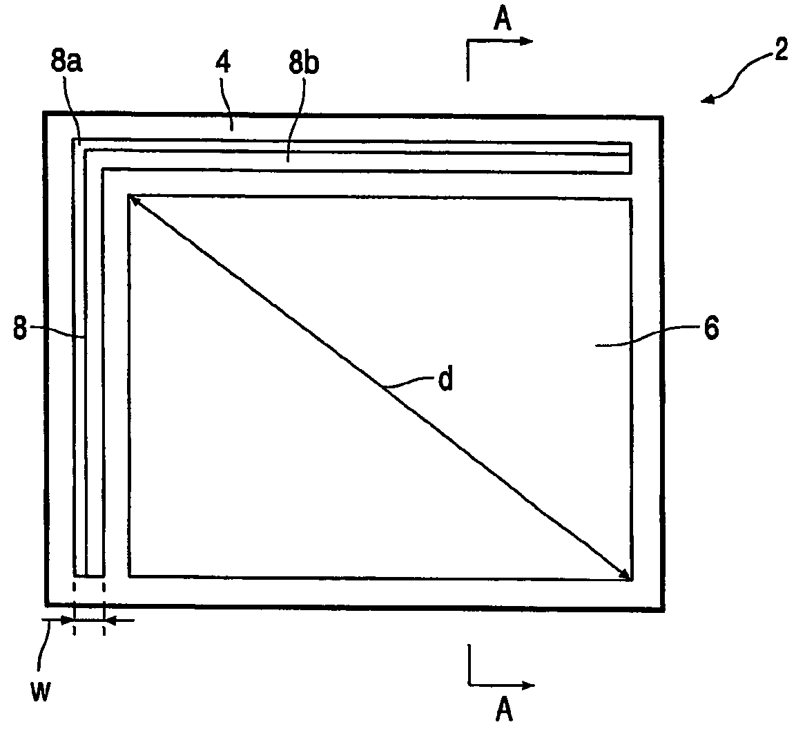
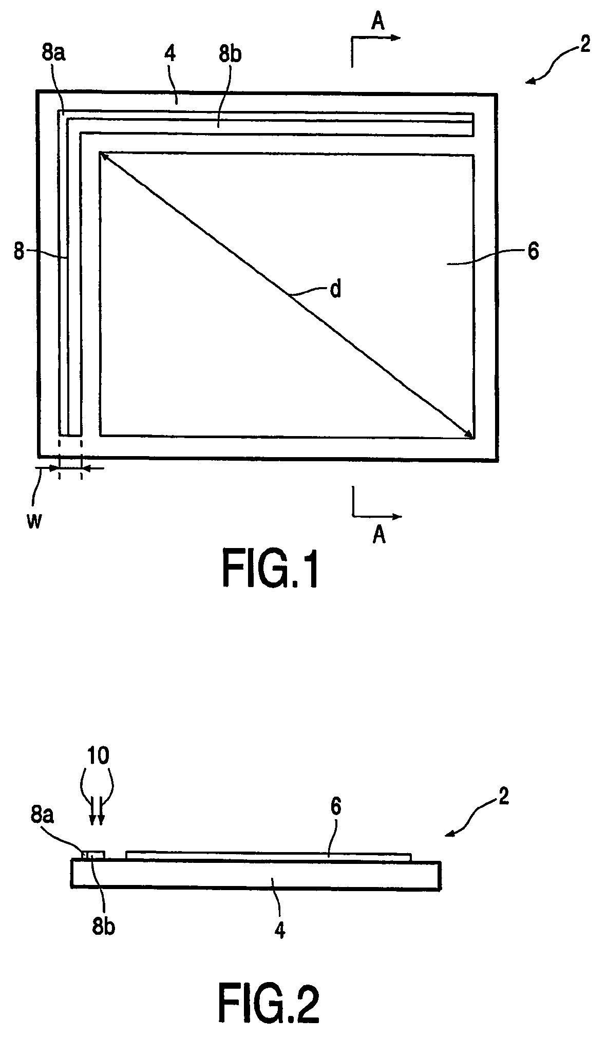
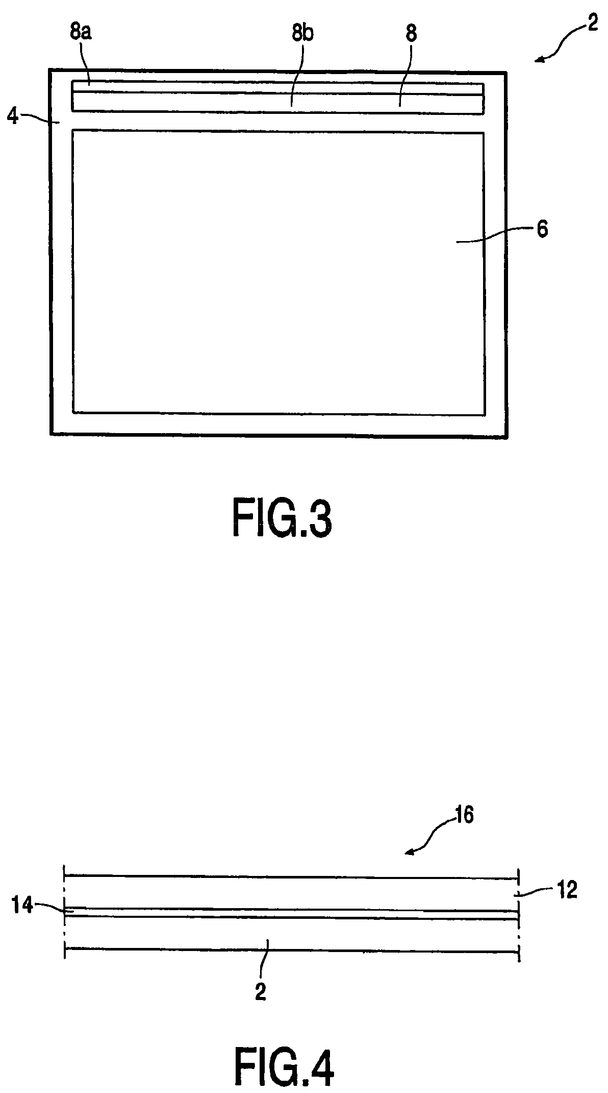
[0037]The active plate 2 of FIG. 1 comprises a substrate 4 for use in an active matrix display, typically formed of glass. On the upper surface thereof are defined a rectangular pixel area 6 and an adjacent peripheral drive circuit area 8 formed of circuitry for driving pixels making up the pixel area. Leads connecting to the substrate and interconnecting the drive and pixel areas are omitted for clarity in the Figure. The width, w, of the elongate peripheral drive circuit area extending along two sides of the pixel area may typically be of the order of 5 mm. The length, d, of a diagonal across the pixel area may vary from around 60 mm for smaller displays used in handheld devices, up to around 430 mm or more for desktop or LC-TV displays. It can therefore be seen that the drive circuit area 8 is a small fraction of the combined area of the pixel and drive circuit areas. As only the drive circuit area or a proportion of it need be subjected to a laser annealing process in accordance...
PUM
 Abstract
Description
Claims
Application Information