Method of fabricating semiconductor device

a semiconductor device and fabrication method technology, applied in semiconductor devices, instruments, photomechanical treatment, etc., can solve the problems of difficult detection of focal points at the time of exposure in real time in a similar method, detection errors may occur, and problems tend to become conspicuous, and achieve high-quality patterns.

Inactive Publication Date: 2009-06-09
RENESAS ELECTRONICS CORP
View PDF22 Cites 0 Cited by
  • Summary
  • Abstract
  • Description
  • Claims
  • Application Information

AI Technical Summary

Benefits of technology

[0016]The present invention has been achieved to solve these problems and an object thereof is to provide a semiconductor device fabrication method capable of forming a highly accurate pattern.
[0018]According to the present invention, the focal point detection light is radiated on the second film including a photosensitive material, and a specified polarized light obtained from the focal point detection light is used, and therefore, it is possible to secure the reflectivity of specified surface boundaries while suppressing the reflectivity of the other surface boundaries such as the upper and lower surface boundaries of the second film at a low value. As a result, the effect of the light reflected from the surface boundaries other than the specified surface boundaries can be suppressed, thereby making it possible to improve the detection accuracy of the focal point at the time of exposure. Thus, the exposure accuracy is improved and a highly accurate pattern can be formed.

Problems solved by technology

In the liquid immersion lithography, the liquid exists on a resist, and therefore it is difficult to detect the focal point at the time of exposure in real time in a method similar to the aforementioned case.
Part of the detection light, however, enters films formed on the substrate and interferes by multiplex reflection in each thin film.
For this reason, a position lower than the uppermost surface of the substrate may be detected on the one hand, and since the detection light is periodically changed due to the effect of multiplex reflection in the underlying thin films, a detection error may occur on the other hand.
This problem tends to become conspicuous in the liquid immersion lithography.
Nevertheless, a similar problem is encountered inherently in the normal exposure in the air.
In a case where the difference is reduced between the refractive index on an exposure medium constituted of a liquid and the refractive index on the resist as in the liquid immersion lithography, therefore, it becomes difficult to increase the reflectivity of the uppermost surface of the substrate (the surface boundary between the exposure medium and the resist, for example).
As a result, a greater amount of detection light intrudes into the resist at the time of detecting the focal point, and the detection light interferes by multiplex reflection on internal reflection surfaces.
As compared with the normal exposure, therefore, detection accuracy of the focal point is liable to be deteriorated.
Reduction in detection accuracy of the focal point at the time of exposure poses problems that the exposure accuracy is reduced and the high-accuracy pattern formation is hampered.

Method used


Image

  • Method of fabricating semiconductor device
  • Method of fabricating semiconductor device
  • Method of fabricating semiconductor device

Examples


first embodiment

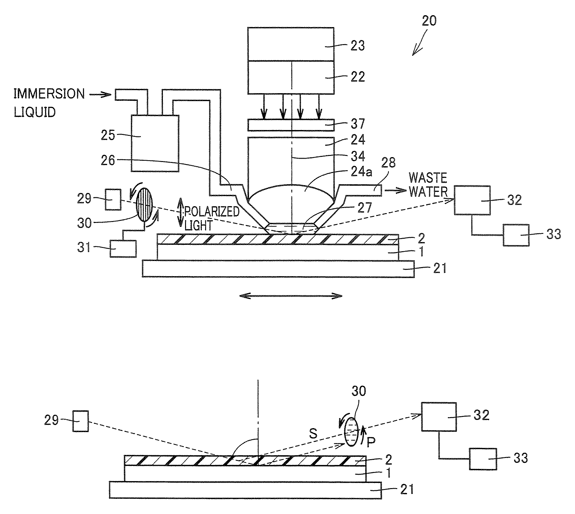
[0049]FIG. 1A is a diagram showing a general configuration of a liquid immersion lithography unit 20 according to the first embodiment of the invention. Liquid immersion lithography unit 20 according to the first embodiment may be an exposure apparatus of step-and-scan type, step-and-repeat type or other types.

[0050]The use of liquid immersion lithography unit 20 as in the first embodiment can meet the requirements for fabrication of a semiconductor device with the design rule of, for example, not more than 45 nm, and makes it possible to form a resist pattern of about not more than 130 nm. In the first embodiment, an application of the invention to a liquid immersion lithography unit. Nevertheless, the present invention is applicable also to an exposure apparatus other than the liquid immersion lithography unit.

[0051]As shown in FIG. 1A, liquid immersion lithography unit 20 according to the first embodiment includes an illumination optical system 22 having an exposure light source ...

second embodiment

[0116]Next, a second embodiment of the invention is explained with reference to FIGS. 19 to 24.

[0117]In the first embodiment described above, an anti-reflection film such as BARC having the ability to absorb the focal point detection light (450 nm to 850 nm) is used for the layer lower than the resist film. In the second embodiment, on the other hand, an upper layer film (top coating material) higher in refractive index than the resist film is formed on the resist film. This upper layer film, being alkali soluble and capable of absorbing the focal point detection light (450 nm to 850 nm), can be formed of a film high in refractive index. The other components are basically similar to the corresponding ones of the first embodiment.

[0118]FIG. 19 shows an example of the film structure on substrate 1 according to the second embodiment. As shown in FIG. 19, the film structure according to the second embodiment includes silicon oxide film 3 of 200 nm formed on the main surface of substrate...

third embodiment

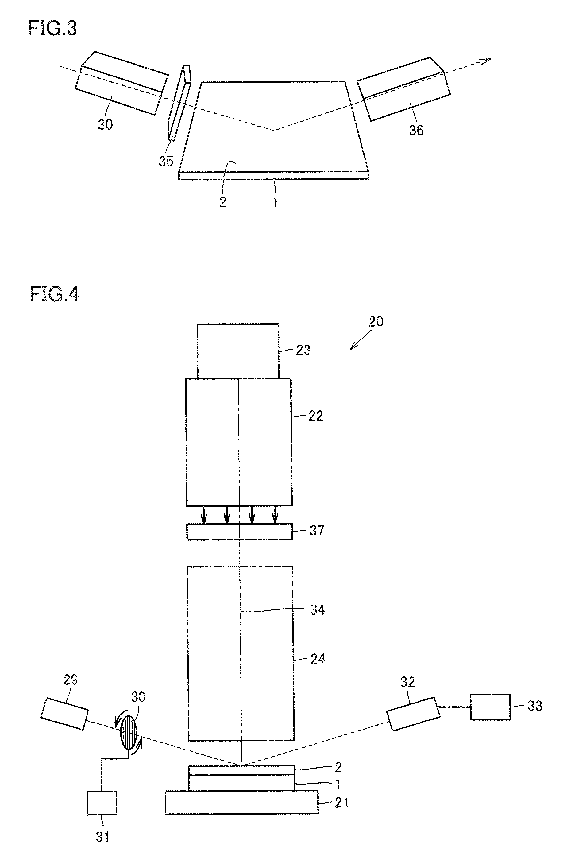
[0136]Next, a third embodiment of the invention is explained. According to the third embodiment, the configuration of the focal point detection unit for detecting the focal point at the time of exposure is different from that of exposure apparatus 20 according to the first embodiment. The other component parts are basically similar to those of the first embodiment.

[0137]As shown in FIG. 3, according to the third embodiment, a photoelastic modulator 35 is interposed between polarizer 30 and substrate 1, and an analyzer 36 is inserted between substrate 1 and light detector 30 (FIG. 1). Also, the third embodiment uses, as the detection light, a linearly polarized light at 45° with the angle of incidence and wavelength as variables. A similar polarizer to that of the first embodiment is usable as polarizer 30. Analyzer 36 includes optical elements such as a polarizing plate, lens, prism and multichannel CCD capable of handling the incidence angle and the wavelength as variables to detec...


PUM


Abstract

An insulating film is formed on a main surface of a substrate. A conductive film is formed on the insulating film. A lower layer resist film, an intermediate layer, an anti-reflection film and an upper layer resist film are formed on the conductive film. A focal point at a time of exposure is detected by detecting a height of the upper layer resist film. In detecting the focal point at the time of exposure, a focal point detection light is radiated on the upper layer resist film. After detecting the focal point, the upper layer resist film is exposed and developed thereby to form a resist pattern. With the resist pattern as a mask, the intermediate layer and the anti-reflection film are patterned, and the lower layer resist film is developed. With these patterns as a mask, the conductive film is etched thereby to form a gate electrode.

Description

BACKGROUND OF THE INVENTION[0001]1. Field of the Invention[0002]The present invention relates to a method of fabricating a semiconductor device, and in particular to a semiconductor device fabrication method capable of forming a highly accurate pattern by detecting a focal point at a time of exposure with high accuracy.[0003]2. Description of the Background Art[0004]In a conventional exposure apparatus, the focal point at the time of exposure is detected by guiding a detection light at a wide angle to a surface of a substrate constituting an object to be measured and thus increasing a reflectivity of the uppermost surface of the substrate. A light reflected from the substrate is detected by a light detector, and a position of the reflected light is measured thereby to detect the focal point at the time of exposure.[0005]In recent years, a new exposure technique called the liquid immersion lithography has come to be closely watched. The liquid immersion lithography is a technique of ...

Claims


Application Information

Patent Timeline
Patent Type & Authority Patents(United States)
IPC IPC(8): H01L21/28H01L21/308
CPCG03F7/70341G03F9/7026G03F9/7065H01L21/28035H01L21/32139H01L29/6659Y10S438/95Y10S438/952G03F7/2041
Inventor ISHIBASHI, TAKEO
Owner RENESAS ELECTRONICS CORP
Why Eureka
Try Eureka