Supercharge Your Innovation With Domain-Expert AI Agents!

Capacitive single-electron transistor

a single-electron transistor, capacitive technology, applied in the direction of superconductor devices, instruments, semiconductor/solid-state device details, etc., can solve the problem that the measurement of the state of quantum bits in superconducting nano-structures has been at least equally difficult as computing operations, and achieves high precision and integration density.

Active Publication Date: 2009-06-23
MAGIQ TECH INC
View PDF5 Cites 6 Cited by
  • Summary
  • Abstract
  • Description
  • Claims
  • Application Information

AI Technical Summary

Benefits of technology

[0014]Besides appreciable sensitivity, the C-SET detector of the present invention has the substantial benefit of absence of internal energy losses and internal noise sources. This means that the C-SET detector only minimally interferes with the quantum system being measured and is thus suitable for surveying and utilizing weak quantum mechanical phenomena. The C-SET detector of the present invention can also be produced in a size smaller than current phase meters by several orders of magnitude, thus allowing high precision and integration density.

Problems solved by technology

Measurement of the state of quantum bits in superconducting nano-structures has proved at least equally difficult as their use for computing operations.

Method used


Image

  • Capacitive single-electron transistor
  • Capacitive single-electron transistor
  • Capacitive single-electron transistor

Examples


Embodiment Construction

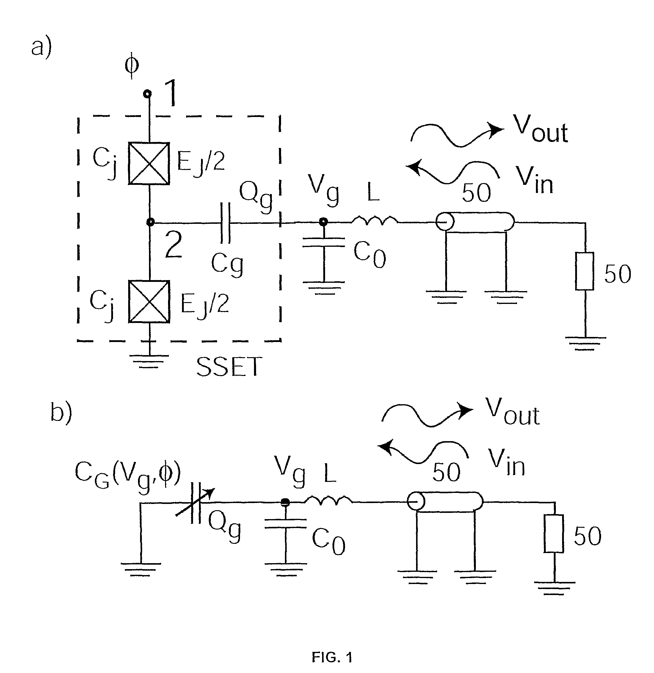
Single-electron transistor SET

[0023]Phenomena occurring on a scale under one micrometer are usually referred to as mesoscopic phenomena. The size of individual atoms, a number of Angstroms, is still several orders of magnitude smaller. However, quantum mechanical phenomena can be detected at low temperatures in mesoscopic electroconductive metal or semiconductor structures. In the case of superconducting metal structures, the scale is less than one degree Kelvin. The term mesoscopic can roughly be used as a synonym of the word nano.

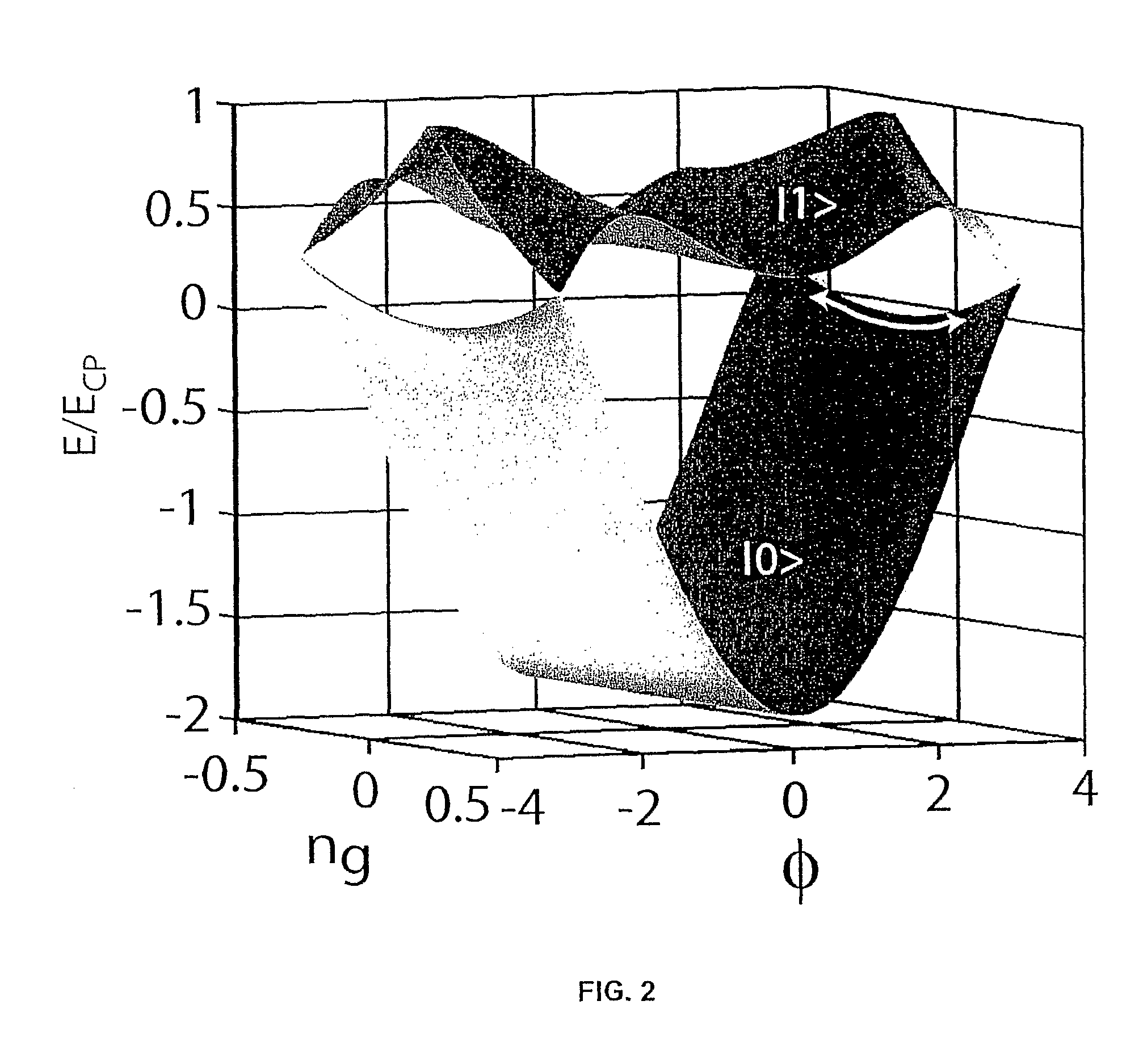
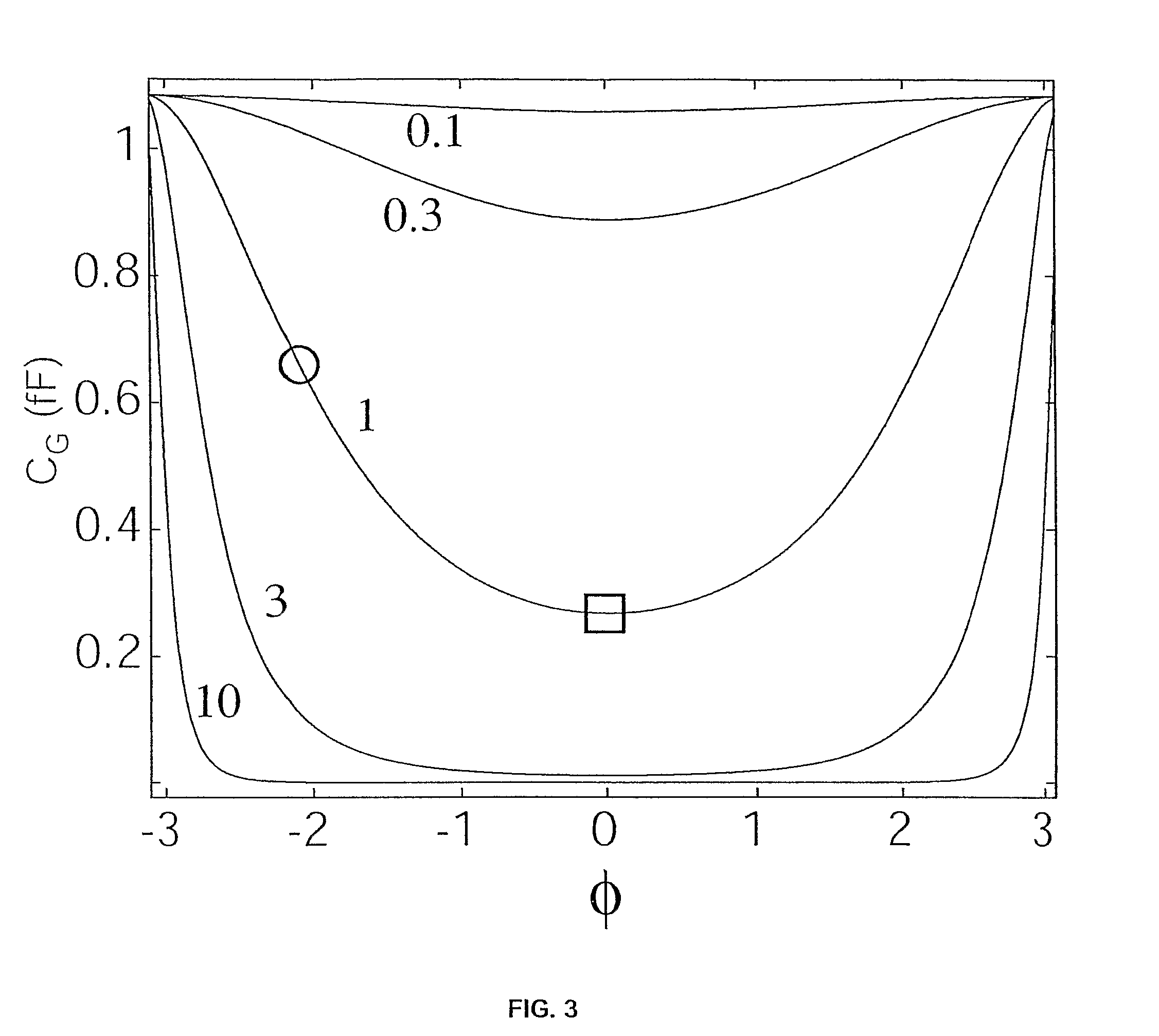
[0024]The mesoscopic basic instrument is the single-electron transistor (SET), which consists of two tunnel junctions having a cross-sectional area of about 10,000 square nanometres. The sum capacitance of these tunnel junctions, which is marked with the symbol CΣ, is of the order of magnitude of a femtofarad. If the charge energy ECP=(2e)2 / 2CΣ of the Cooper pair is much above the temperature, i.e. ECP>>kBT, the SET acts as the most sensitive electric cha...


PUM


Abstract

The invention is a sensitive measuring instrument, which is principally applied to quantum computation, especially to measurement of quantum bits consisting of superconducting micro and nano-structures. The state of a quantum bit is expressed as the voltage-time integral over a circuit component. Phase measurement is performed by measuring the capacitance of a single-electron transistor between the gate and ground.

Description

CLAIM OF PRIORITY[0001]This application hereby claims priority under 35 USC §119 based on Finnish patent application serial no. Fl 20041000, entitled “Kapasitiivinen yhden elektronin transistori,” filed on Jul. 19, 2004, and having issued on January 20, 2006 as Finnish Patent No. 117032B, which patent application and patent are incorporated by reference herein.FIELD OF THE INVENTION[0002]The invention is a sensitive measuring instrument principally implemented in the domain of quantum computation, especially in the measurement of quantum bits consisting of superconducting micro and nano-structures.BACKGROUND ART[0003]Whereas a bit, the basic unit of digital electronics, always has the value 0 or 1 because of binary logic, a quantum bit, the basic unit of quantum calculation, may be a random combination, i.e. a superposition of the values 0 and 1. The mathematic expression of the state of a quantum bit is a|0>+b|1>, in which a and b are complex numbers meeting the equation |a|2...

Claims


Application Information

Patent Timeline
IPC IPC(8): G01R29/00H01L29/06H10N60/12G06N99/00H01L
CPCB82Y10/00G06N99/002G06N10/00
Inventor HAKONEN, PERTTISILLANPAA, MIKAROSCHIER, LEIF
Owner MAGIQ TECH INC
Features
  • R&D
  • Intellectual Property
  • Life Sciences
  • Materials
  • Tech Scout
  • Unparalleled Data Quality
  • Higher Quality Content
  • 60% Fewer Hallucinations
Learn More