Multi-band LC resonance voltage-controlled oscillator with adjustable negative resistance cell

a voltage-controlled oscillator and negative resistance technology, applied in pulse generators, pulse techniques, modulation, etc., can solve the problems of increasing the phase noise of the voltage-controlled oscillator, and the difficulty of integrating a wide-band lc resonance voltage-controlled oscillator in a multi-band multi-mode wireless transceiver, so as to suppress phase noise and suppress noise

Inactive Publication Date: 2009-06-30
ELECTRONICS & TELECOMM RES INST
View PDF21 Cites 23 Cited by
  • Summary
  • Abstract
  • Description
  • Claims
  • Application Information

AI Technical Summary

Benefits of technology

[0011]Also, the present invention is directed to a wide-band LC resonance voltage-controlled oscillator, which suppresses phase noise caused by a tail current source that is adopted for controlling fluctuation in oscillation amplitude.
[0012]Further, the present invention is directed to a wide-band LC resonance voltage-controlled oscillator, which suppresses noise caused by a tail current source while compensating for oscillation amplitude.

Problems solved by technology

It is difficult to embody a wide-band LC resonance voltage-controlled oscillator in a multi-band multi-mode wireless transceiver.
However, the tail current source 190 brings about low- and high-frequency thermal noise, thus increasing the phase noise of the LC resonance voltage-controlled oscillator.

Method used


Image

  • Multi-band LC resonance voltage-controlled oscillator with adjustable negative resistance cell
  • Multi-band LC resonance voltage-controlled oscillator with adjustable negative resistance cell
  • Multi-band LC resonance voltage-controlled oscillator with adjustable negative resistance cell

Examples


exemplary embodiment 1

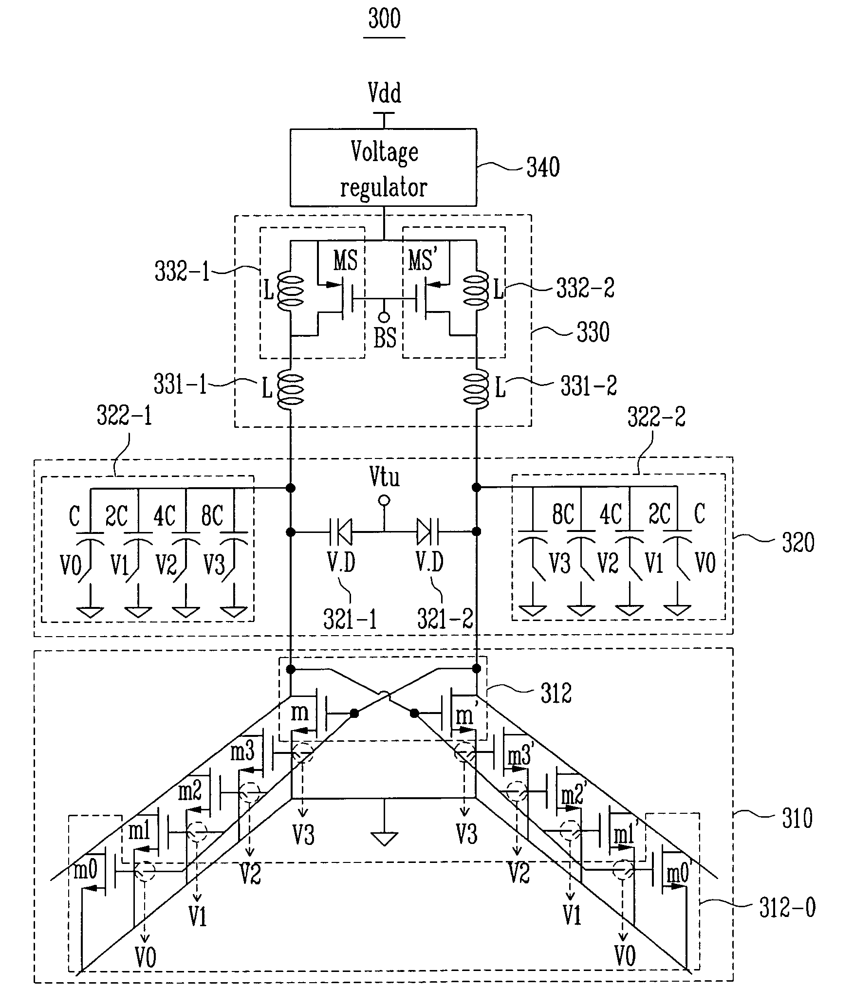
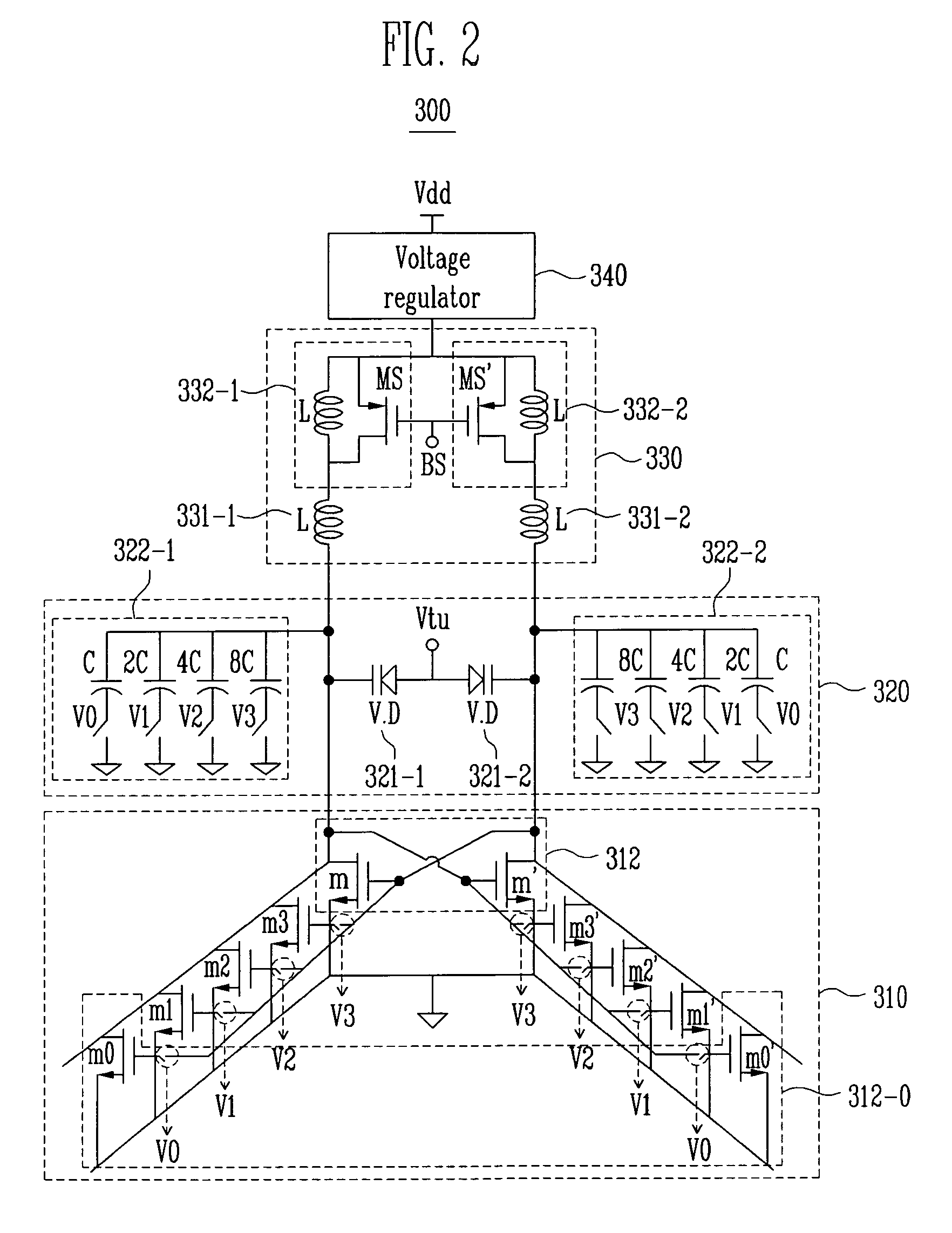
[0024]FIG. 2 is a circuit diagram of a wide-band LC resonance voltage-controlled oscillator 300 according to an exemplary embodiment of the present invention.

[0025]Referring to FIG. 2, the LC resonance voltage-controlled oscillator 300 includes an inductor 330, a capacitor 320, a discrete negative resistance cell 310, and a voltage regulator 340. Specifically, the inductor 330 provides an inductance element and the capacitor 320 provides a capacitance element that together determine the frequency of an oscillation wave. The discrete negative resistance cell 310 provides a discretely determined negative resistance element to keep the amplitude of the oscillation wave constant. Also, the voltage regulator 340 keeps a voltage applied from a power supply voltage terminal to the inductor 330 constant.

[0026]The inductor 330 includes a first inductor 332-1 and 331-1 and a second inductor 332-2 and 331-2, which are connected to the voltage regulator 340 and have different current paths. The...

exemplary embodiment 2

[0043]FIG. 4 is a circuit diagram of a wide-band LC resonance voltage-controlled oscillator 301 including an emitter-degeneration coupled pair 352 in addition to a negative resistance cell 350 according to another exemplary embodiment of the present invention.

[0044]Referring to FIG. 4, the LC resonance voltage-controlled oscillator 301 includes a voltage regulator 340, an inductor 330, first and second discrete capacitors 322-1 and 322-2, and first and second varactors 321-1 and 321-2, which perform almost the same functions as those of FIG. 2. A first inductor 332-1 and 331-1, the first discrete capacitor bank 322-1, and the first varactor 321-1 form one LC oscillation path, while a second inductor 332-2 and 331-2, the second discrete capacitor bank 322-2, and the second varactor 321-2 form the other LC oscillation path.

[0045]In the present exemplary embodiment, the LC resonance voltage-controlled oscillator 301 is structurally characterized by the emitter-degeneration coupled pair...

exemplary embodiment 3

[0051]FIG. 5 is a circuit diagram of a wide-band LC resonance voltage-controlled oscillator 302 with an adjustable emitter-degeneration negative resistance cell 360 according to still another exemplary embodiment of the present invention.

[0052]Referring to FIG. 5, the negative resistance cell 360 includes a plurality of unit discrete negative resistance cells that are connected in parallel in response to control bit signals V0˜V3. Each of the unit discrete negative resistance cells 362-0 is comprised of a pair of unit MOS transistors m, m′, m0, m0′, ˜m3, and m3′, a unit resistor, and a unit capacitor. The pair of unit MOS transistors m, m′, m0, m0′, ˜m3, and m3′ are configured as an emitter-degeneration coupled pair in which one drain is connected to the other source, and have drains connected to a connection node between an inductor and a discrete capacitor bank. The unit resistor is connected in series to the pair of unit MOS transistors m, m′, m0, m0′, ˜m3, and m3′, and the unit ...


PUM


Abstract

Provided is an LC resonance voltage-controlled oscillator (VCO) used for a multi-band multi-mode wireless transceiver. In order to generate a multi-band frequency, a capacitor bank and a switchable inductor are included in the LC resonance voltage-controlled oscillator. The LC resonance voltage-controlled oscillator employs an adjustable emitter-degeneration negative resistance cell in place of tail current sources in order to compensate for non-uniform oscillation amplitude caused by the capacitor bank and prevent the degradation of a phase noise due to the tail current sources. The LC resonance voltage-controlled oscillator includes an inductor providing an inductance element partially determining the frequency of an oscillation wave; a discrete capacitor bank providing a capacitance element partially determining the frequency of the oscillation wave and being discretely determined by a control bit signal; and a discrete negative resistance cell providing a negative resistance element that is discretely determined by the control bit signal, to keep the amplitude of the oscillation wave constant.

Description

CROSS-REFERENCE TO RELATED APPLICATION[0001]This application claims priority to and the benefit of Korean Patent Application Nos. 2005-119516, filed Dec. 8, 2006, and 2006-55270, filed Jun. 20, 2006, the disclosures of which are incorporated herein by reference in their entirety.BACKGROUND[0002]1. Field of the Invention[0003]The present invention relates to a multi-band inductor-capacitor (LC) resonance voltage-controlled oscillator (VCO) and, more specifically, to a multi-band LC resonance voltage-controlled oscillator that operates in a multi-band multi-mode and compensates for fluctuation in the amplitude of an oscillation wave.[0004]2. Discussion of Related Art[0005]It is difficult to embody a wide-band LC resonance voltage-controlled oscillator in a multi-band multi-mode wireless transceiver. Nowadays, capacitor banks 122-1 and 122-2 and varactors 121 are mounted in an LC resonance portion with a fixed inductor 130 as shown in FIG. 1, in order to extend the frequency adjustment...

Claims


Application Information

Patent Timeline
Patent Type & Authority Patents(United States)
IPC IPC(8): H03B7/06H03C3/22H03L1/00
CPCH03B5/1228H03B5/1215H03B5/1243H03B5/1265H03B5/1271H03B2201/0208H03B2201/0266H03J2200/10H03B5/08
Inventor LEE, JA YOLKIM, KWI DONGKWON, CHONG KIKIM, JONG DAELEE, SANG HEUNGCHO, KYOUNG IK
Owner ELECTRONICS & TELECOMM RES INST
Why Eureka
Try Eureka