Integrated circuit device and low noise block down converter including same
a low noise block and integrated circuit technology, applied in the direction of ghz frequency transmission, substation equipment, broadcasting with distribution, etc., to achieve the effect of reducing the leakage of input signals and low noise block down converters
- Summary
- Abstract
- Description
- Claims
- Application Information
AI Technical Summary
Benefits of technology
Problems solved by technology
Method used
Image
Examples
embodiment 1
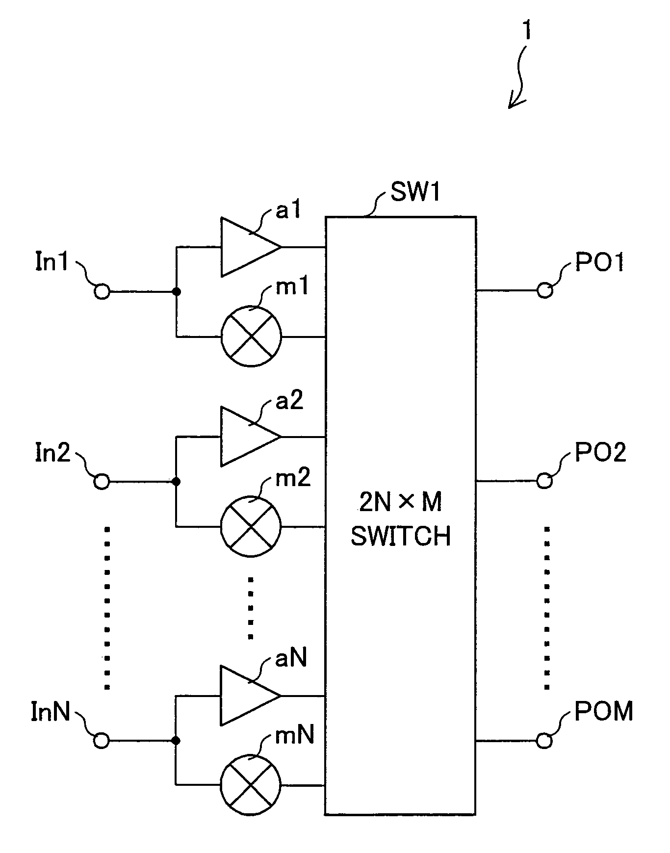
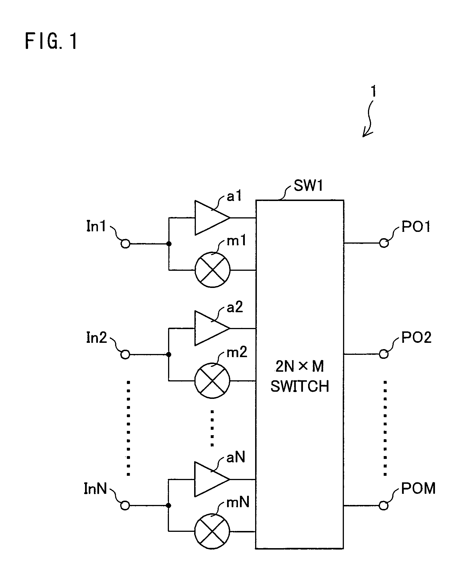
[0067]The following will describe an embodiment of the present invention in reference to figures. Described below is a case where an integrated circuit device (hereinafter, switch block) of the present invention is a part of a signal recombination circuit of a LNB.
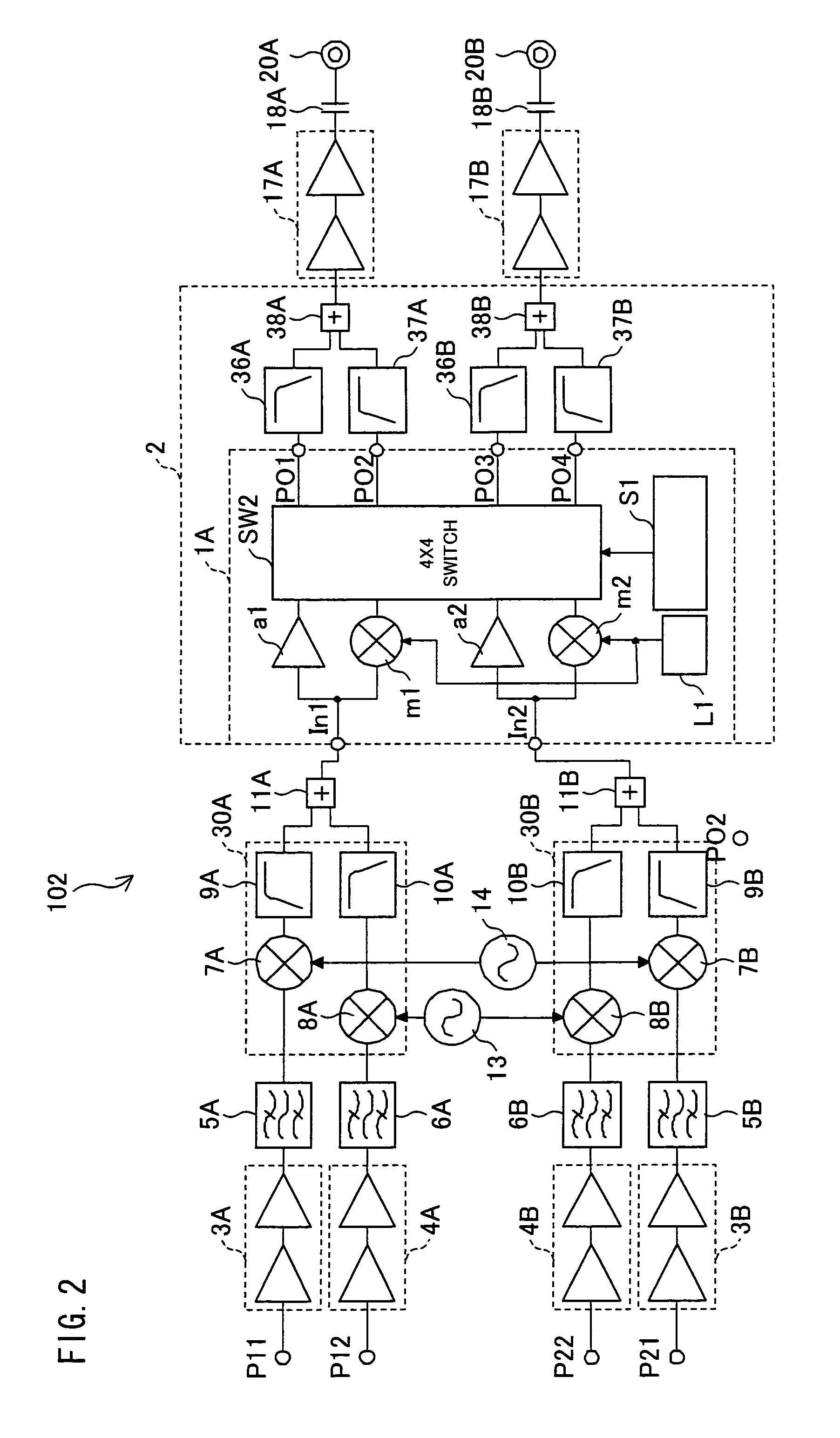
[0068]FIG. 2 is a circuit diagram of a LNB 102, in which the signal recombination circuit 55 in FIG. 13 is replaced by a signal recombination circuit 2 of the present embodiment. Since the circuit configuration of the LNB 102 has already been described in Background of the Invention, the description thereof is omitted. Also, members having the same functions are given the same numbers, unless otherwise stated.
[0069]The signal recombination circuit 2 receives a first synthesized signal and a second synthesized signal. Since the first and second synthesized signals are generated in the same manner as the aforesaid first and second synthesized signal in the conventional art, the description thereof is omitted.
[0070]As shown i...
embodiment 2
[0139]FIG. 10 outlines a switch block 1B in a signal recombination circuit 2 of another embodiment of the present invention. It is noted that members having the same numbers as those in the switch block 1A have the same functions, unless otherwise stated.
[0140]As shown in the figure, the switch block 1B includes low noise amplifiers (LNAs) lna1 and lna2, amplifiers a1 and a2, mixers m1 and m2, a 4×2 switch circuit SW5, a local signal generator L1, and a control device S1. Input terminals In1 and In2 are input terminals of the switch block 1B, whereas output terminals PO1 and PO2 are output terminals of the switch block 1B.
[0141]The low noise amplifier lna1 subjects, to low noise amplification, the first synchronized signal supplied to the input terminal In1. The low noise amplifier lna2 subjects, to low noise amplification, the second synchronized signal supplied to the input terminal In2. The 4×2 switch circuit SW5 is an example of the 2N×M switch circuit SW1.
[0142]The following wi...
PUM
 Abstract
Description
Claims
Application Information


