System for controlling an overlay, method for controlling overlay, and method for manufacturing a semiconductor device
a technology of overlay control and manufacturing method, applied in the field of photolithography, can solve the problem of not being able to satisfy the overlay accuracy with respect to other underlying layers at the same tim
- Summary
- Abstract
- Description
- Claims
- Application Information
AI Technical Summary
Benefits of technology
Problems solved by technology
Method used
Image

Examples
first embodiment
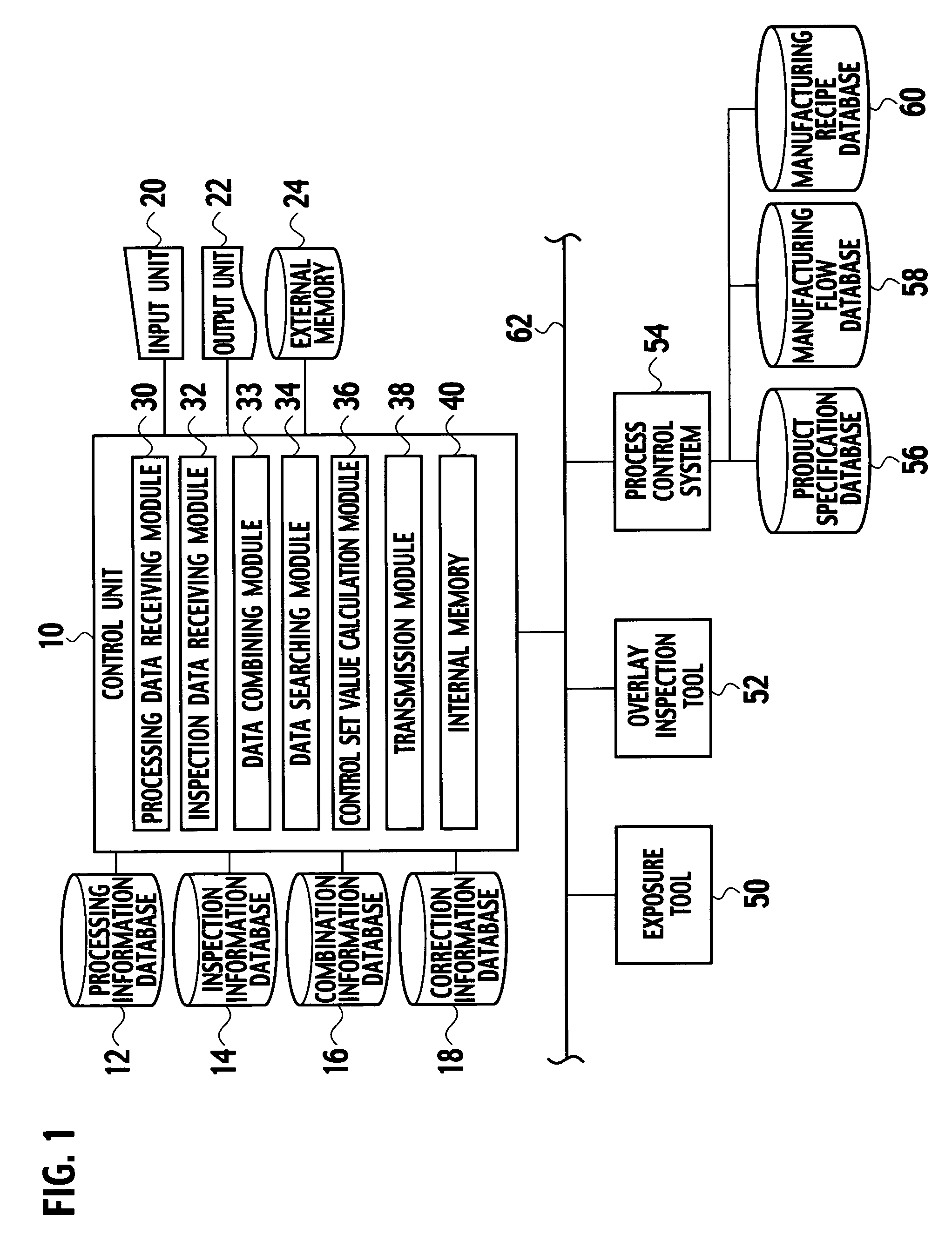
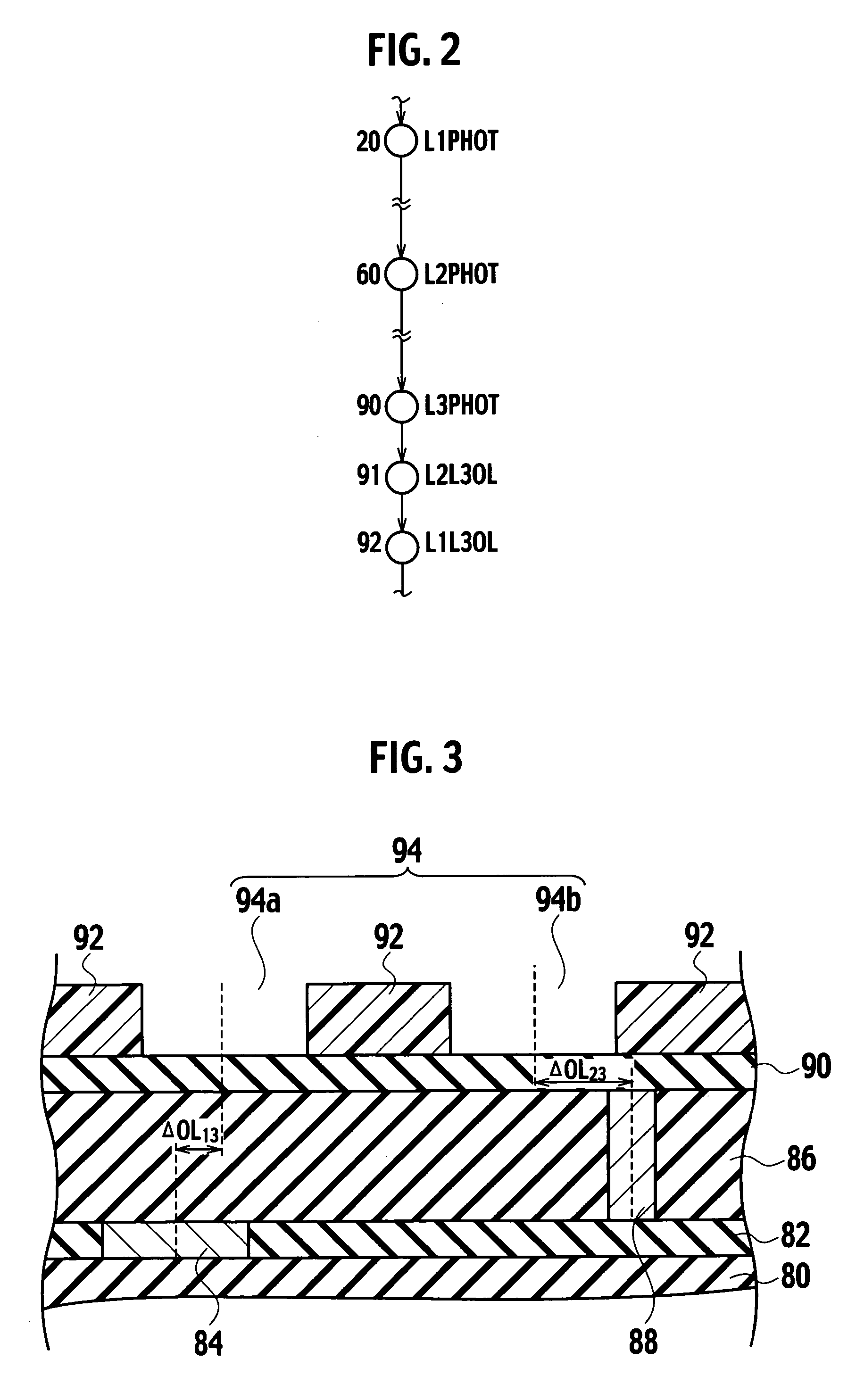
[0029]As shown in FIG. 1, a system for controlling an overlay according to a first embodiment of the present invention includes a control unit 10, a processing information database 12, an inspection information database 14, a combination information database 16, a correction information database 18, an input unit 20, an output unit 22, an external memory 24, and the like. The control unit 10 includes a processing data receiving module 30, an inspection data receiving module 32, a data combining module 33, a data searching module 34, a control set value calculation module 36, a transmission module 38, an internal memory 40, and the like. An exposure tool 50, an overlay inspection tool 52, a process control system 54, and the like, are connected to the control unit 10 by way of a communication line 62, such as a local area network (LAN). A product specification database 56, a manufacturing flow database 58, a manufacturing recipe database 60 and the like, are connected to the process ...
second embodiment
Modification of Second Embodiment
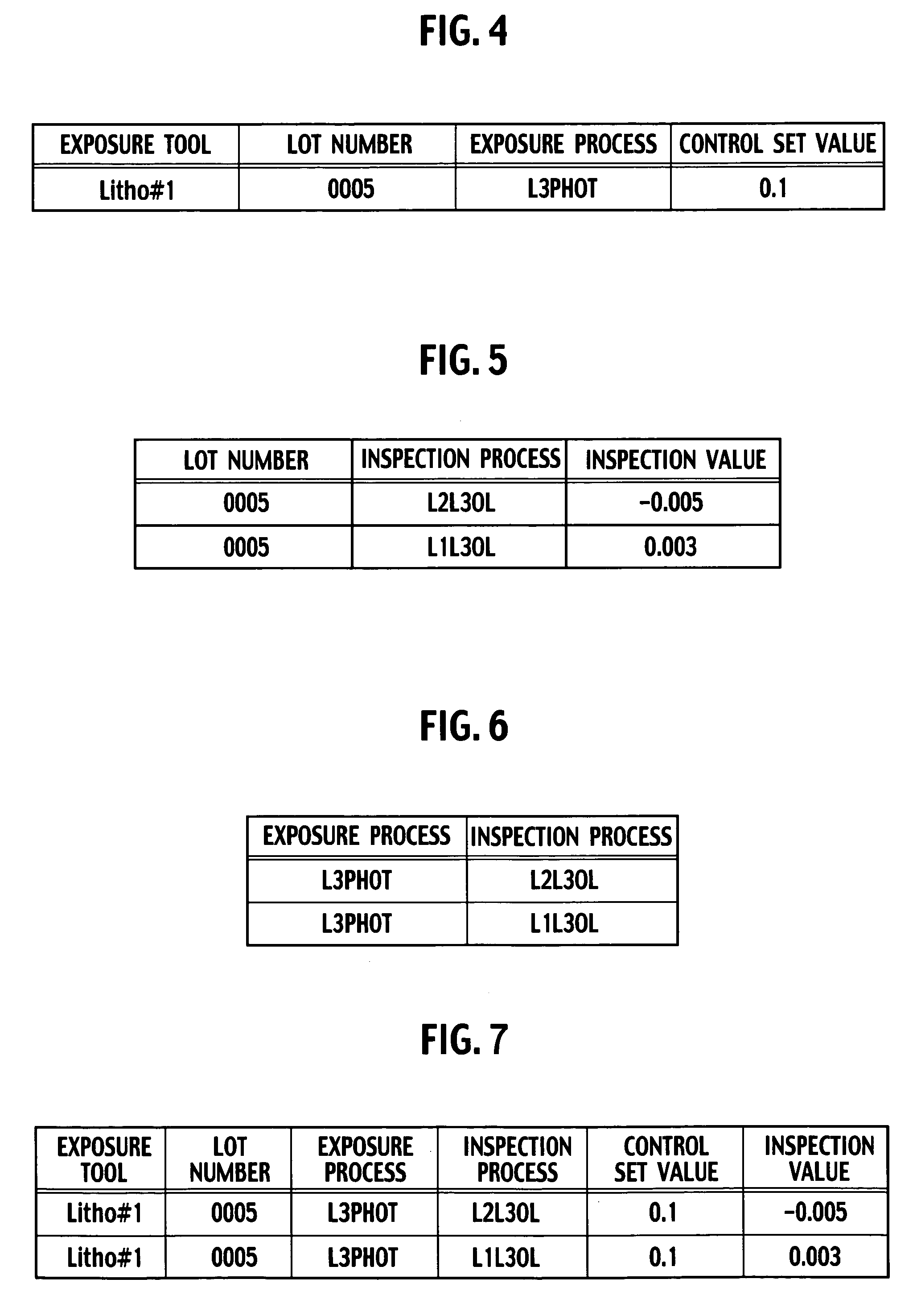
[0082]In a method for controlling an overlay according to a modification of the second embodiment of the present invention, a pattern of a transferred layer is defined by different overlay accuracies in the X and Y directions in an underlying layer. For example, control set values x and y of the X and Y directions are described as “0.1” and “0.2”, respectively, in the processing data string stored in the processing information database 12, shown in FIG. 11. As shown in FIG. 15, the control set values x and y are described as “0.005” and “0.006” with respect to the inspection process name L2L3OL, and as “0.007” and “0.008” with respect to the inspection process name L1L3OL, respectively, in the processing data string stored in the inspection information database 14. As shown in FIG. 16, the exposure process name, the inspection process name, the control set value of the X and Y directions, the inspection value of the X and Y directions, and the like, ...
PUM
| Property | Measurement | Unit |
|---|---|---|
| weight | aaaaa | aaaaa |
| weight calculation | aaaaa | aaaaa |
| weights | aaaaa | aaaaa |
Abstract
Description
Claims
Application Information
 - R&D
- Intellectual Property
- Life Sciences
- Materials
- Tech Scout
- Unparalleled Data Quality
- Higher Quality Content
- 60% Fewer Hallucinations
Browse by: Latest US Patents, China's latest patents, Technical Efficacy Thesaurus, Application Domain, Technology Topic, Popular Technical Reports.
© 2025 PatSnap. All rights reserved.Legal|Privacy policy|Modern Slavery Act Transparency Statement|Sitemap|About US| Contact US: help@patsnap.com