VSB receiver and carrier recovery apparatus thereof

a receiver and carrier recovery technology, applied in the field of digital tv, can solve the problems of low power of i signal from complex multiplier, data jitter,

Inactive Publication Date: 2009-07-07
LG ELECTRONICS INC
View PDF10 Cites 11 Cited by
  • Summary
  • Abstract
  • Description
  • Claims
  • Application Information

AI Technical Summary

Benefits of technology

[0044]An object of the present invention is to provide a VSB receiver and a carrier recovery apparatus thereof, in which a pilot signal component can be easily extracted by automatically controlling a bandwidth of a filter for filtering a pilot signal component passing through a transmission channel when a carrier wave is recovered using a VSB modulated signal.

Problems solved by technology

In the case of the FPLL that is dependent on the pilot, data component except the pilot component does not provide information necessary for the carrier recovery and also causes a jitter due to data after the carrier recovery.
Meanwhile, if the component of the pilot signal is severely weak, even the LPF having the wide bandwidth cannot easily extract the pilot component.
However, if the pilot signal is damaged due to the channel, power of the I signal from the complex multiplier becomes very weak near the DC.
Therefore, in the system which performs the carrier recovery based on the pilot signal, its performance is degraded and thus the carrier cannot be recovered.
If the LPF having the narrow bandwidth is simply used to extract the pilot signal, it is impossible to solve the problems occurring when the carrier frequency offset exists.

Method used


Image

  • VSB receiver and carrier recovery apparatus thereof
  • VSB receiver and carrier recovery apparatus thereof
  • VSB receiver and carrier recovery apparatus thereof

Examples


first embodiment

[0088]FIG. 7 is a block diagram of a carrier recovery part of a digital TV receiver according to the present invention.

[0089]Referring to FIG. 7, the carrier recovery part of the digital TV receiver includes a complex multiplier 701, a first band pilot signal and frequency / phase error detecting part 718, a second band pilot signal and frequency / phase error detecting part 719, a comparing part 712, a selecting part 713, a loop filter 714, and a VCO (or an NCO) 715.

[0090]The complex multiplier 701 receives an I signal and a Q signal from a delay unit (not shown) and a Hilbert transformer (not shown), multiplies the I signal and the Q signals by an output signal of the VCO 715, and outputs a baseband I signal and a baseband Q signal (carrier wave). The first band pilot signal and frequency / phase error detecting part 718 includes first and second LPFs 702 and 703 having a first bandwidth, a first delay unit 704, a first code detector 705, a first multiplier 706, and a first integrator 7...

second embodiment

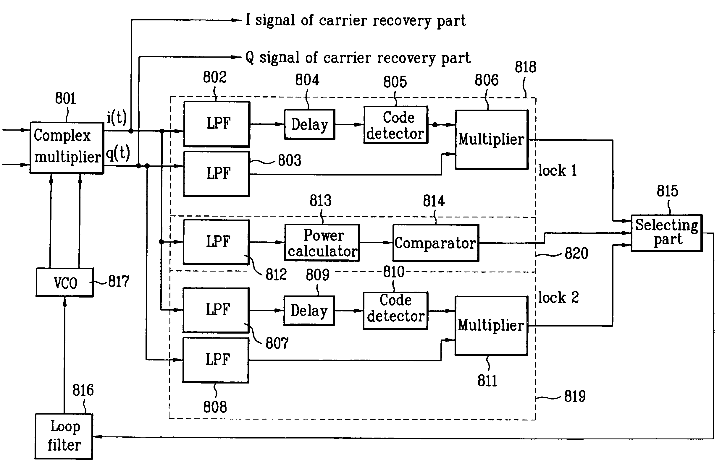
[0104]FIG. 8 is a block diagram of a carrier recovery part of a digital TV receiver according to the present invention.

[0105]Referring to FIG. 8, the carrier recovery part of the digital TV receiver includes a complex multiplier 801, a first frequency / phase error detecting part 818, a second frequency / phase error detecting part 819, a pilot power comparing part 820, a selecting part 815, a loop filter 816, and a VCO 817.

[0106]The complex multiplier 810 receives an I signal and a Q signal from a delay unit (not shown) and a Hilbert transformer (not shown), multiplies the I signal and the Q signals by an output signal of the VCO (or NCO) 817, and outputs a baseband I signal and a baseband Q signal (carrier wave). The first frequency / phase error detecting part 818 includes first and second LPFs 802 and 803 having a first bandwidth, a first delay unit 804, a first code detector 805, and a first multiplier 806. The first frequency / phase error detecting part 818 detects a first frequency / ...

third embodiment

[0110]FIG. 9 is a block diagram of a carrier recovery part of a digital TV receiver according to the present invention.

[0111]Referring to FIG. 9, the carrier recovery part of the digital TV receiver includes a complex multiplier 901, a first band signal filtering part 914, a second band signal filtering part 915, a selecting part 906, a power calculating part 907, a comparing part 908, a frequency / phase error detecting part 916, a loop filter 912, and a VCO (or NCO) 913.

[0112]The complex multiplier 810 receives an I signal and a Q signal from a delay unit (not shown) and a Hilbert transformer (not shown), multiplies the I signal and the Q signals by an output signal of the VCO (or NCO) 913, and outputs a baseband I signal and a baseband Q signal (carrier wave). The first band signal filtering part 914 includes first and second LPFs 902 and 903 having a first bandwidth and filters a signal component except the I and Q signal components of the first band among the baseband signals out...


PUM


Abstract

There are provided a VSB receiver and a carrier recovery apparatus thereof, in which a carrier is recovered using a VSB modulated signal. In the VSB receiver, a digital processing part selects a desired channel frequency through an antenna, converts the channel frequency into an intermediate frequency, and digitalizes the channel frequency by passing a predetermined band of the intermediate frequency. A carrier recovery part extracts pilot signals by using a first LPF having a first bandwidth and a second LPF having a second bandwidth, and recovers a baseband carrier wave signal from a passband signal by using one of the extracted pilot signals. A clock demodulation part removes the pilot signal from the baseband carrier wave signal and extracts a synchronizing signal. A noise removing part removes a linear noise and a residual phase jitter of the baseband signal by using the synchronizing signal. A decoding part decodes the baseband signal whose noise is removed. Accordingly, the carrier recovery can be stably performed even when the pilot signal is weak.

Description

[0001]This application claims the benefit of the Korean Application Nos. 10-2003-0086336, filed on Dec. 1, 2003, and 10-2003-0094592, filed on Dec. 22, 2003 which are hereby incorporated by reference.BACKGROUND OF THE INVENTION[0002]1. Field of the Invention[0003]The present invention relates to a digital TV, and more particularly, to a VSB receiver and a carrier recovery apparatus thereof, in which a carrier is recovered using a VSB modulated signal.[0004]2. Discussion of the Related Art[0005]A vestigial sideband (VSB) system of Grand Alliance is adopted as the standard for a transmission system of digital TV (e.g., HDTV) in the United States and Korea. In the VSB system, when a signal is amplitude-modulated, upper and lower sidebands are generated based on a carrier wave. At this point, when one of the two sidebands is greatly reduced, the other sideband is modulated. That is, only one sideband spectrum of a baseband signal is removed to a passband and then transmitted, such that ...

Claims


Application Information

Patent Timeline
Patent Type & Authority Patents(United States)
IPC IPC(8): H04L27/22H04L27/14H03D1/24H04L1/00H04L27/00H04L27/06H04N5/38H04N5/44H04N5/455
CPCH03D1/24H04L27/066H04N5/455H04L1/004H04L2027/0028H04L2027/0057H04L2027/0069H04L2027/0087H04N5/38H04N5/4401H04L2027/0067H04N21/426
Inventor KIM, JOON TAEKIM, TOK
Owner LG ELECTRONICS INC
Why Eureka
Try Eureka