This helps you quickly interpret patents by identifying the three key elements:
Problems solved by technology
Method used
Benefits of technology
Benefits of technology
[0026]An object of the present invention is to provide an electroluminescent device capable of realizing a high reliability and a long-term service life which are major problems to be solved, and suppressing an after-image phenomenon frequently occurring in liquid crystal displays.
[0029]The present inventor has examined to solve the above-described problems, and found that it becomes possible to realize a long-term service life of an electroluminescent device while keeping a high luminance, even if the device has a conventional structure using conventional materials, by optimizing a drive waveform applied thereto.
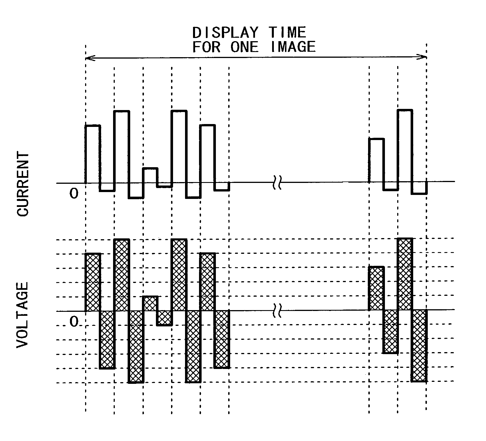
[0031]On the other hand, in a practical method of driving an electroluminescent device, as is well known, a ratio of a light emission time to a one image display period, that is, a duty ratio is desirable to be increased for enhancing the luminous intensity even with the same applied waveform intensity, and is also desirable to be decreased to some extent for increasing a dark (non-light emitting) state per one image display period in order to suppress an after-image phenomenon upon display of a moving picture and thereby sharpening the image quality.
[0044]It may be considered that light emission be due to the flow-in of electrons between electrodes of an electroluminescent device, whereas the deterioration of the device be due to ion species. Such ion species are bulky and therefore very small in mobility. Further, if a high frequency drive waveform is applied to an electroluminescent device, ion species little occur by electrode reaction, that is, by ionization of a metal material for forming an electrode. From this viewpoint, preferably, the one image display period is divided into a plurality of sets of the light emitting periods and the non-light emitting periods. With this configuration, since a high frequency drive waveform is applied to the device, it is possible to further improve the deterioration of the device. It is to be noted that since the mobility of ion species is due to the magnitude and applied time of an electric field between electrodes, it is required to make the intensity of a forward electric field equal to the intensity of a reverse electric field for preventing occurrence of ion migration in practice.
Liquid crystal displays, however, have problems that the viewing angle is narrow, the power consumption of a back light is large under a dark environment because of the use of no spontaneous light, the response to high-speed video signals of high definition is insufficient although such a response characteristic is expected to be put to practical use in future, and an after-image phenomenon occurs.
In particular, liquid crystal displays with large screen sizes have a further problem that the production costs are raised because of difficulties in producing such large-sized liquid crystal displays.
Such displays, however, are also high in production costs and have difficulties in forming a matrix structure of light-emitting diodes on one substrate.
Accordingly, displays of this type have a problem to be solved before the displays are put to practical use as low-cost substitutes for CRTs.
Such a direct current drive or a single polarity pulse drive of an organic EL device is liable to cause device deterioration for the following reasons (1), (2) and (3).
(1) Polarization of migratable ion species, which are contained as impurities in a device structure, in a single layer or between electrodes, to incidentally or inevitably deteriorate the device.
(2) Ionization of an element originally contained in an electrode material by application of an electric field, followed by elution of the element as migratable ions in the device structure, to change the electric field state of a layer structure precisely designed, thereby causing device deterioration.
The former drive method, however, has a problem that since an organic EL device is driven by current control with its luminous intensity specified, if a resistance change occurs, it fails to sufficiently cope therewith.
In other words, such a drive method is disadvantageous in that the condition of optimization of an asymmetric waveform is unclear.
The former drive method is intended to cause light emission in band regions of both polarities of a bipolar waveform, and if a device has a substantially ideal device structure with the enhanced luminous efficiency, a diode rectifying characteristic is improved; however, since light emission occurs at the time of reverse bias, the device may be significantly deterioration.
A method of suppressing device deterioration by applying a voltage in the direction reversed to that of a DC voltage between an anodeelectrode and a cathodeelectrode has been disclosed in Japanese Patent No. 3169974; however, this document does not sufficiently examine the optimization of the magnitude and timing of the voltage in the direction reversed to that of the DC voltage.
Method used
Image
Click on the blue label to locate the original text in one second.
Reading with bidirectional positioning of images and text.
Examples
examples 1-9
[0143]In each of these examples, the organic EL device having the device structure 1 was driven with current control based on a rectangular bipolar type current waveform shown in FIG. 15A.
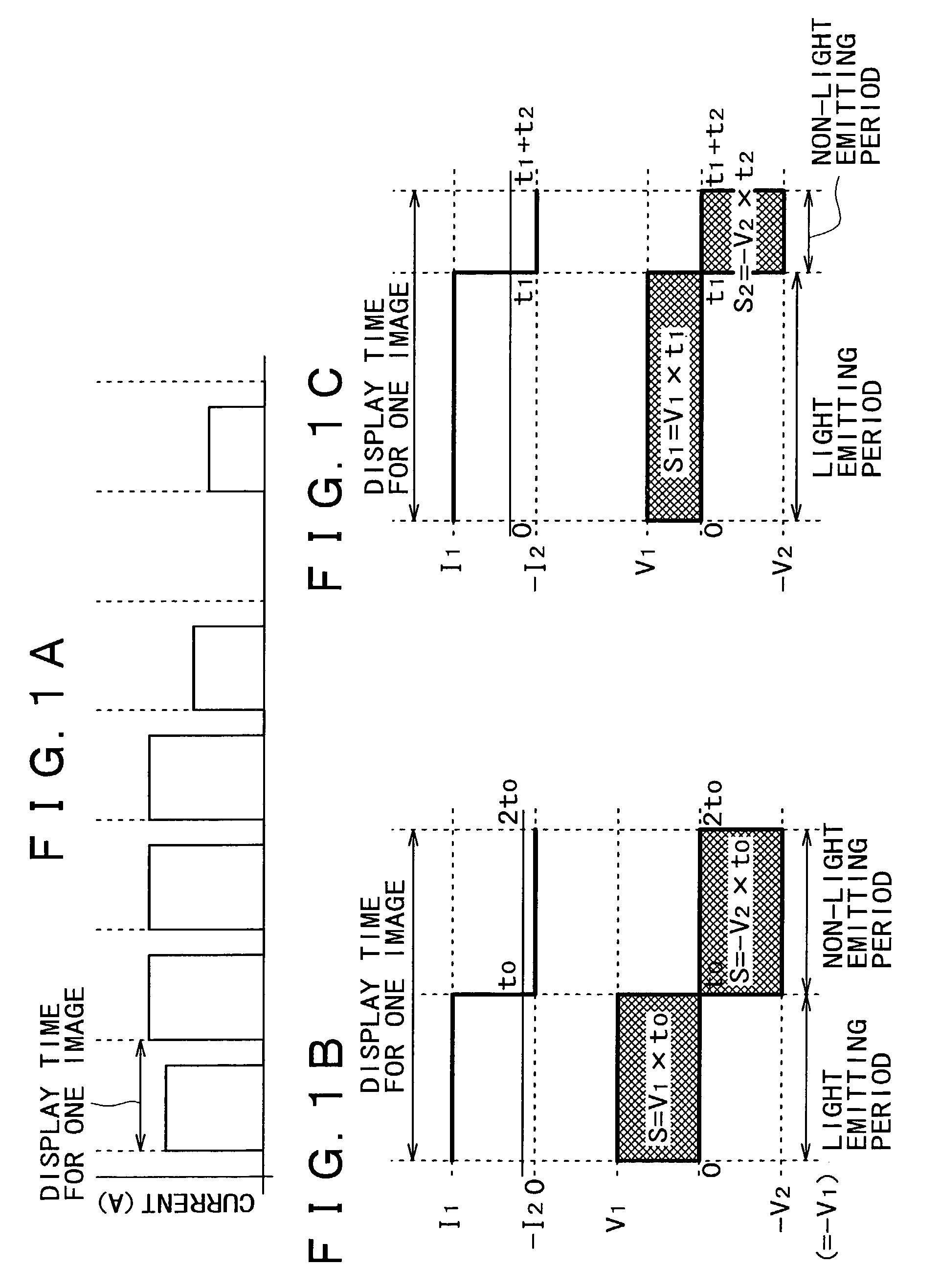
[0144]As shown in FIG. 15A, a one image display period was taken as 16.7 ms at a frequency of 60 Hz, whereby an image display time in the one image display period was in a range of 0 to 16.7 ms.
[0145]The duty ratios were set to 5%, 10%, 30%, 50%, 70%, 75%, 80%, 90%, and 95% for Examples 1 to 9, respectively, whereby the one image display period in each of Examples 1 to 9 was divided into 5% (10%, 30%, 50%, 70%, 75%, 80%, 90%, 95%) of a light emitting period and 95% (90%, 70%, 50%, 30%, 25%, 20%, 10%, 5%) of a non-light emitting period. With such a duty ratio, the initial luminance became 100 cd / m2.
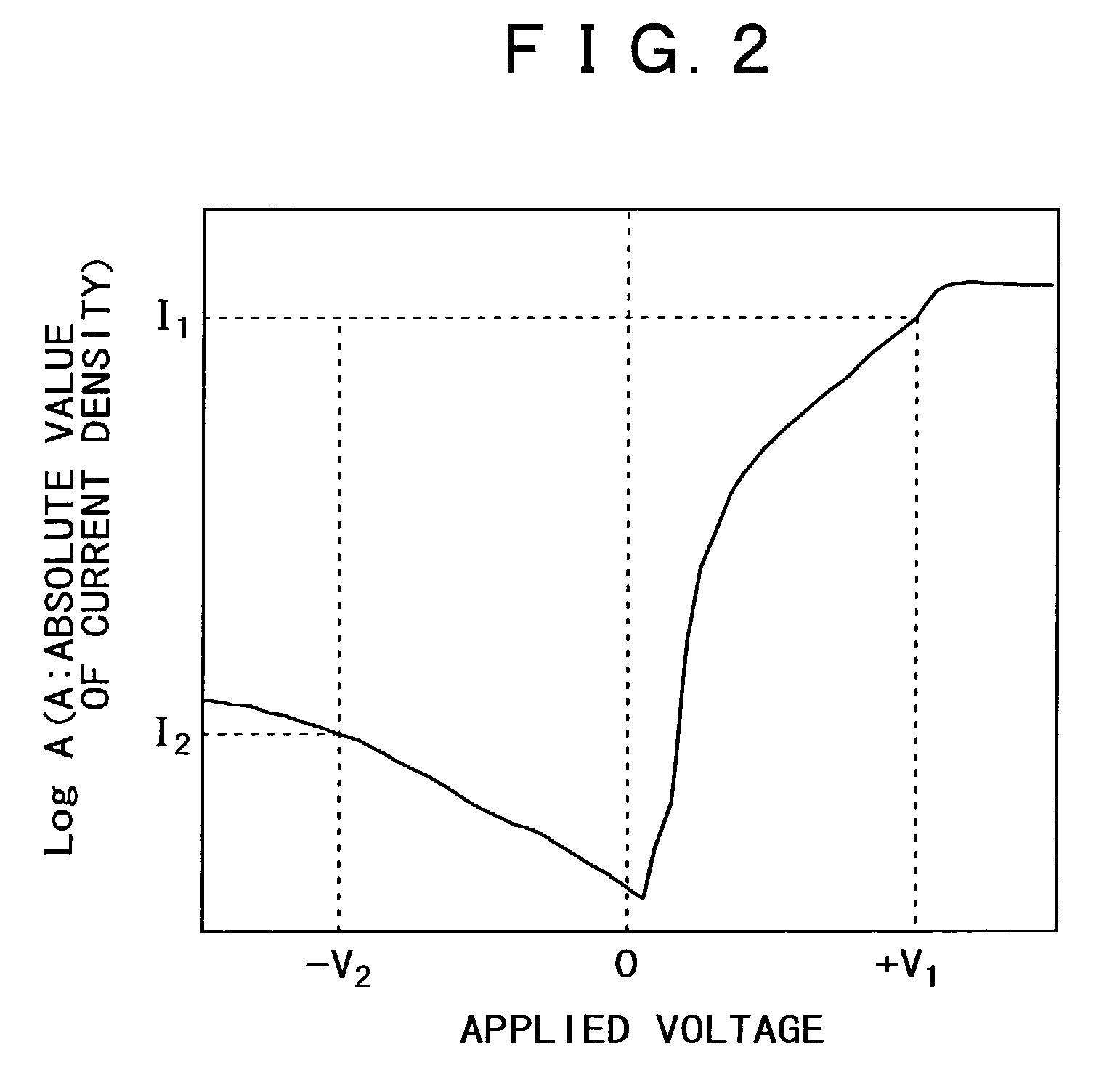
[0146]Further, in each of Examples 1 to 9, the waveform was set to a rectangular bipolar type current waveform shown in FIG. 15A. To be more specific, a current value in the non-light emitting period was ...
examples 10 to 12
[0154]In each of these examples, the organic EL device having the device structure 1 was driven with current control based on a rectangular bipolar type current waveform shown in FIG. 16A.
[0155]As shown in FIG. 16A, a one image display period was taken as 16.7 ms at a frequency of 60 Hz, whereby an image display time in the one image display period was in a range of 0 to 16.7 ms.
[0156]The duty ratio was set to 50%, whereby the one image display period was divided into 50% of a light emitting period and 50% of a non-light emitting period, and further, the waveform in the image display period was divided into two for Example 10, into five for Example 11, and divided into ten for Example 12, with the voltage and current values in each waveform kept constant. With such a duty ratio, the initial luminance became 100 cd / m2.
[0157]Further, in each of Examples 10 to 12, the waveform was set to a rectangular bipolar type current waveform shown in FIG. 16A. To be more specific, a current value...
example 13
[0164]In this example, the organic EL device having the device structure 2 was driven with current control based on a rectangular bipolar type current waveform shown in FIG. 17.
[0165]As shown in FIG. 17, a one image display period was taken as 16.7 ms at a frequency of 60 Hz, whereby an image display time in the one image display period was in a range of 0 to 16.7 ms.
[0166]The duty ratio was set to 50%, whereby the one image display period is divided into 50% of a light emitting period and 50% of a non-light emitting period. With this duty ratio of 50%, the initial luminance became 100 cd / m2.
[0167]Further, the waveform was set to a rectangular bipolar type current waveform shown in FIG. 17. To be more specific, a current value in the non-light emitting period was set such that the integral intensity of a voltage that corresponds to a current value in the light emitting period is substantially canceled by the integral intensity of a voltage that corresponds to the current value in th...
PUM
Abstract
An electroluminescent device, in which a layer having a light emitting region is provided between an anode and a cathode, is driven by applying a bipolar waveform as a drive waveform per one image display period to the device. The one image display period is divided into a light emitting period and a non-light emitting period. The bipolar waveform per one image display period is set such that a waveform portion (current or voltage) for generating an electric field reversed to an electric field caused in the light emitting period is applied in the non-light emitting period, and that an integral intensity obtained by multiplying a voltage value by an applied time in the light emitting period is balanced with or canceled by an integral intensity obtained by multiplying a voltage value by an applied time in the non-light emitting period. Since the optimized drive waveform is applied to the electroluminescent device, it is possible to realize a high reliability and a long-term service life of the device.
Description
[0001]This application claims priority to Japanese Patent Application Number JP2002-129540, filed May 1, 2002, which is incorporated herein by reference.BACKGROUND OF THE INVENTION[0002]The present invention relates to a method of driving an electroluminescent device (EL device) configured such that a layer having a light emitting region is provided between an anode and a cathode.[0003]Cathode-ray tubes (CRT) having high luminance and high color reproducibility have been most widely employed as displays; however, they are bulky and heavy, and high in power consumption. On the other hand, lightweight, highly efficient flat panel displays have been actively studied and developed, for example, for picture display of computers and television sets.[0004]For example, liquid crystal displays of an active matrix driven type or the like have been put on the market as lightweight, highly efficient flat panel displays.[0005]Liquid crystal displays, however, have problems that the viewing angle...
Claims
Application Information
Patent Timeline
Application Date:The date an application was filed.
Publication Date:The date a patent or application was officially published.
First Publication Date:The earliest publication date of a patent with the same application number.
Issue Date:Publication date of the patent grant document.
PCT Entry Date:The Entry date of PCT National Phase.
Estimated Expiry Date:The statutory expiry date of a patent right according to the Patent Law, and it is the longest term of protection that the patent right can achieve without the termination of the patent right due to other reasons(Term extension factor has been taken into account ).
Invalid Date:Actual expiry date is based on effective date or publication date of legal transaction data of invalid patent.

