Apparatus and method for testing and debugging an integrated circuit

a technology for integrated circuits and apparatuses, applied in the field of apparatus and methods for testing and debugging integrated circuits, system and method for downloading trace information from integrated circuits, can solve the problems of increasing the amount of trace data, reducing the number, and exponentially complex testing of integrated circuits

Inactive Publication Date: 2009-07-14
MARVELL ASIA PTE LTD
View PDF62 Cites 17 Cited by
  • Summary
  • Abstract
  • Description
  • Claims
  • Application Information

AI Technical Summary

Problems solved by technology

One disadvantage of shrinking microelectronics is that the testing of integrated circuits becomes exponentially more complex.
However, such extra functions usually require extra pins (besides the JTAG TAP) to output the resulting data.
One problem with the prior art design is that the trace port and status analyzer 150 uses multiple pins of the SOC for the parallel output of the trace data.
As SOCs become more complex, not only does the total number of I / O pins needed for critical functions increase—thus reducing the number of available pins which can be designated as trace output pins—but also the amount of trace data increases, thus requiring more trace output pins for transferring the increased trace data.
Usually, it is the number of trace output pins that are sacrificed for other uses in integrated circuit design, thereby causing difficulties as well as a bottleneck at the trace port output of the integrated circuit.
However, area on an integrated circuit is in short supply, and using up more area for a trace FIFO buffer is expensive and wasteful.

Method used


Image

  • Apparatus and method for testing and debugging an integrated circuit
  • Apparatus and method for testing and debugging an integrated circuit
  • Apparatus and method for testing and debugging an integrated circuit

Examples


Embodiment Construction

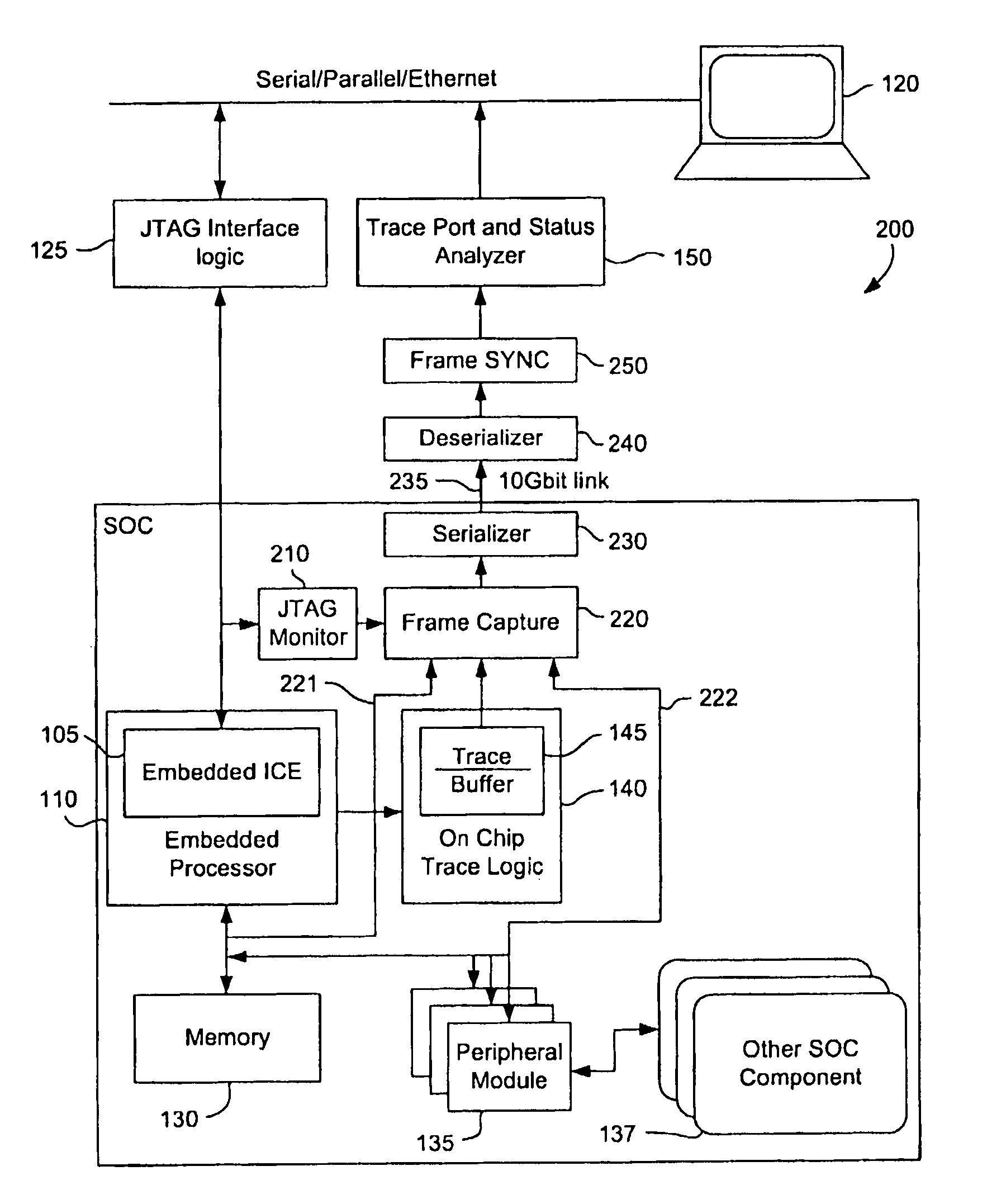
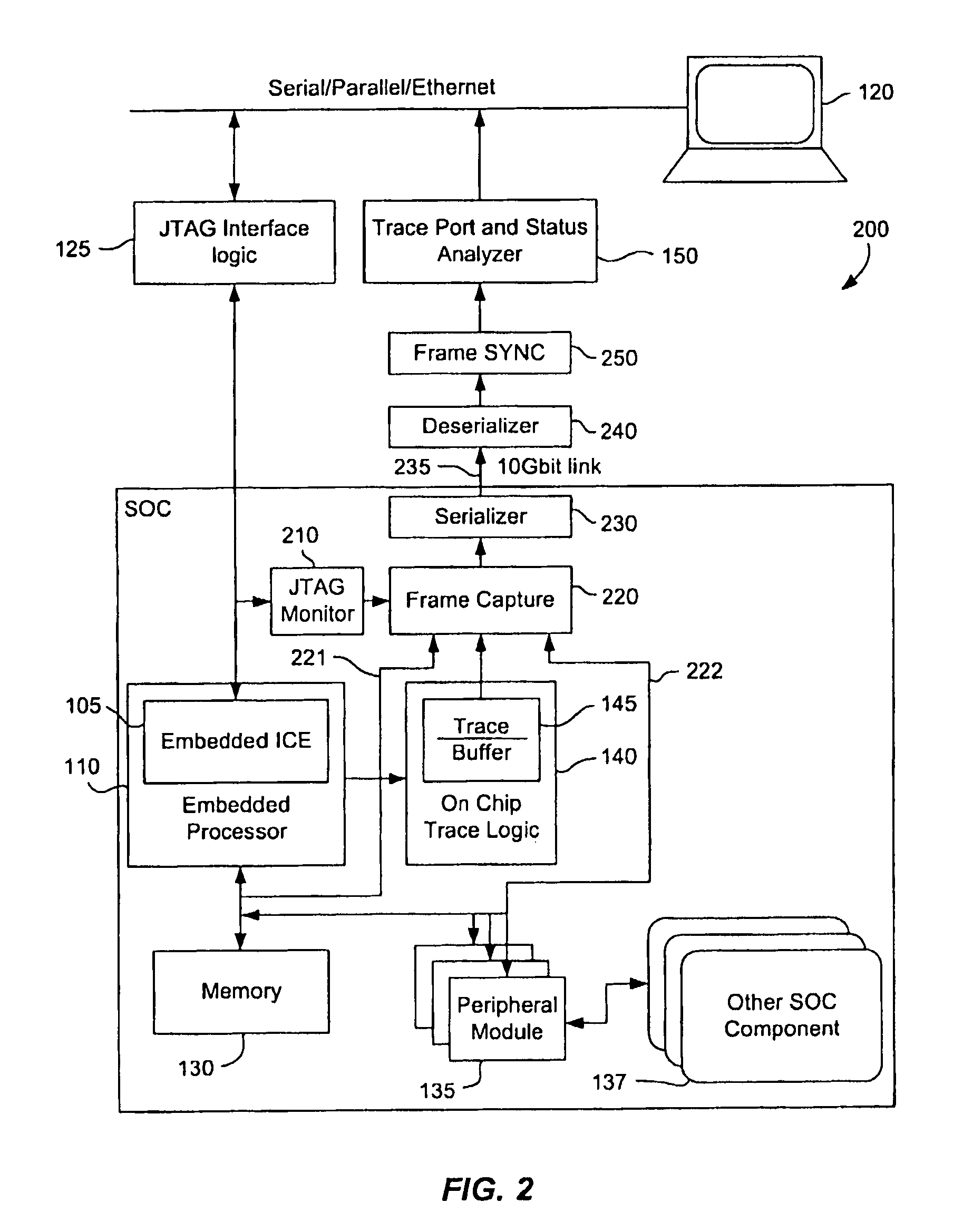
[0026]FIG. 2 shows an SOC 200 with a debugging and emulation system according to a preferred embodiment of the present invention. Similarly to FIG. 1, embedded ICE 105 is located within embedded processor 110. An external debugging and emulation program, located in PC 120, uses the JTAG interface logic 125 (by means of JTAG TAP, not shown here) to access and control ICE 105. ICE 105 can access, control, upload, and download from any memory 130 or peripheral modules 135 which control other SOC components 137. The output of the debugging and emulation is forwarded to trace logic 140 and, more particularly, to trace FIFO (First-In, First-Out) 145.

[0027]Although the preferred embodiment in FIG. 2 uses a JTAG interface 125, it should be understood that the present invention is not limited to such an interface. In fact, any debugging and testing hardware, with or without an emulator, may be used with the present invention. Furthermore, the memory 130 may be any sort of memory, whether vol...


PUM


Abstract

An integrated circuit (IC) comprises an embedded processor. An embedded in-circuit emulator (ICE) emulates at least one function of the embedded processor, performs at least one of testing and debugging on the IC, and generates testing results based on the at least one of the testing and the debugging. A serializer located on the IC receives the testing results from at least one of the embedded ICE and the embedded processor, serializes the testing results, and serially outputs the testing results from the IC.

Description

CROSS-REFERENCE TO RELATED APPLICATIONS[0001]This application is a continuation of U.S. patent application Ser. No. 10 / 375,986 filed Feb. 27, 2003. The disclosure of the above application is incorporated herein by reference.BACKGROUND OF THE INVENTION[0002]1. Field of the Invention[0003]This invention relates generally to testing systems and devices and specifically to a system and method for downloading trace information from an integrated circuit.[0004]2. Description of the Related Art[0005]One disadvantage of shrinking microelectronics is that the testing of integrated circuits becomes exponentially more complex. A convenient and efficient means of testing increasingly complex integrated circuits is to design them with testing hardware already built-in. In 1985, a consortium of European electronics companies formed the Joint Test Action Group (JTAG) in order to create an industry standard which would define an architecture and software protocol for built-in testing hardware. The ...

Claims


Application Information

Patent Timeline
Patent Type & Authority Patents(United States)
IPC IPC(8): G01R31/28
CPCG01R31/31705G06F11/2236G01R31/318572
Inventor AZIMI, SAEEDHO, SON
Owner MARVELL ASIA PTE LTD
Why Eureka
Try Eureka