

Tapered through-silicon via structure
a technology of throughsilicon vias and tapered profiles, which is applied in the direction of semiconductor devices, semiconductor/solid-state device details, electrical devices, etc., can solve the problems of reducing the size of the required size to make these components, requiring more complex designs, and physical limitations of the density that can be achieved in two dimensions, so as to reduce the undercut and improve the sidewall coverage of diffusion barrier layers
- Summary
- Abstract
- Description
- Claims
- Application Information
AI Technical Summary
Benefits of technology
Problems solved by technology
Method used
Image

Examples
Embodiment Construction
[0017]The making and using of the presently preferred embodiments are discussed in detail below. It should be appreciated, however, that the present invention provides many applicable inventive concepts that can be embodied in a wide variety of specific contexts. The specific embodiments discussed are merely illustrative of specific ways to make and use the invention, and do not limit the scope of the invention.
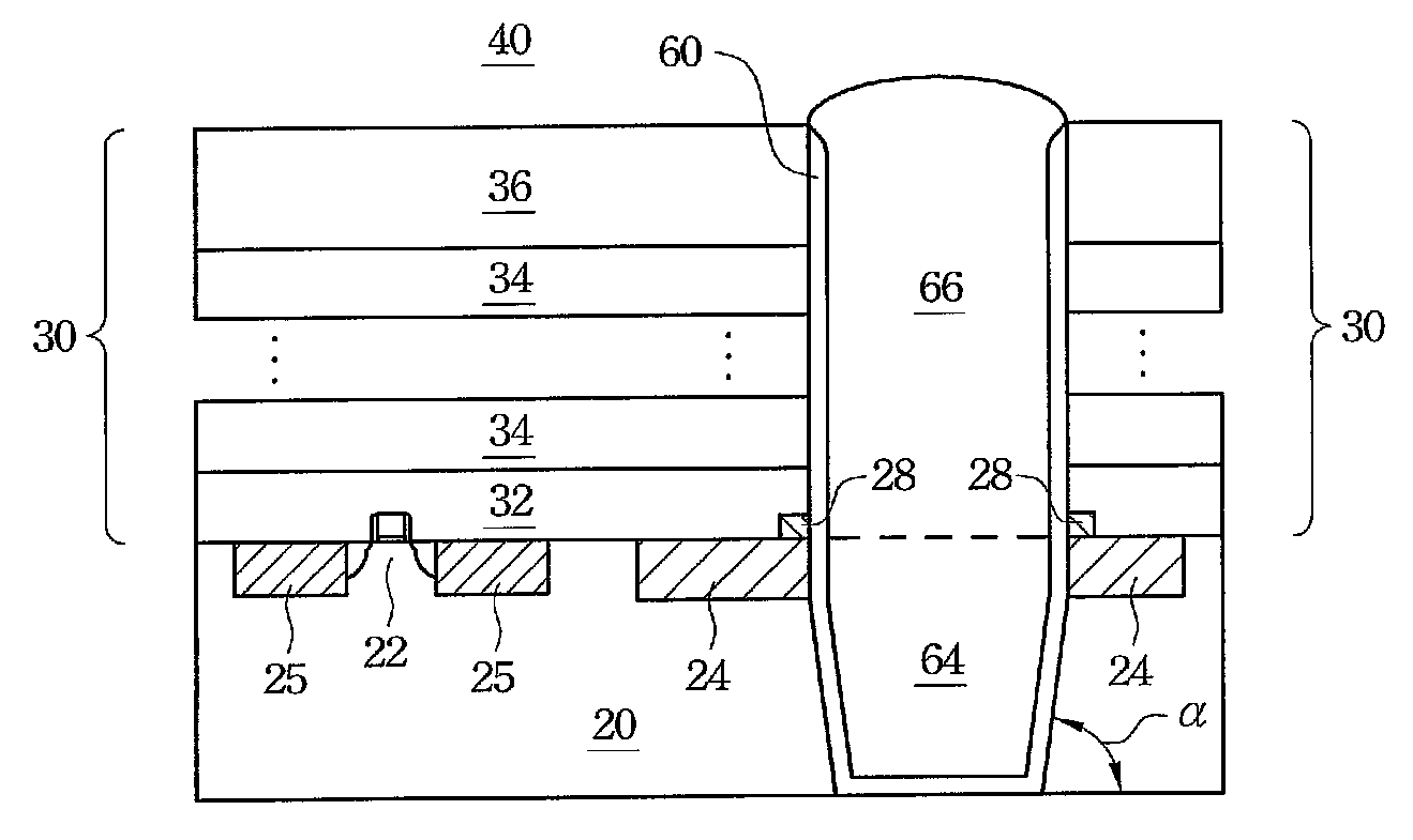
[0018]A novel through-silicon via (TSV) structure and the methods of forming the same are provided. The intermediate stages of manufacturing a preferred embodiment of the present invention are illustrated. The variations of the preferred embodiments are then discussed. Throughout the various views and illustrative embodiments of the present invention, like reference numbers are used to designate like elements.
[0019]Referring to FIG. 3A, substrate 20, which is preferably a silicon substrate, is provided. Substrate 20 may also be formed of other semiconductor materials containi...
PUM
 Abstract
Description
Claims
Application Information