Transfer-ESC based on a wafer

a technology of transfer-esc and wafers, applied in the direction of electric switches, tumbler/rocker switches, electric switches, etc., can solve the problems of brittleness, sensible wafers, and foils that are not reusable, and achieve the effect of current density

Inactive Publication Date: 2009-07-21
RETZLAFF UDO HEINZ
View PDF21 Cites 11 Cited by
  • Summary
  • Abstract
  • Description
  • Claims
  • Application Information

AI Technical Summary

Benefits of technology

[0011]In order to create a high amount of bipolar electrode-unit-cells, thin-film techniques known from the manufacturing process of Integrated Circuits (Chips) are applied. Each electrode-unit-cell, in accordance with the invention, consists of one inside peak-electrode, a lateral insulator layer, one surrounding electrode and a top dielectric layer. It is known that SiO2 has a high breakdown voltage of up to 1000 V per μm. Besides, it is possible to create very pure and defect free silicon dioxide layers which generate only small amounts of leakage currents at 300 degree Celsius. Taking into account that breakdown voltages from 200 V to 2000 V are needed, the width of the lateral insulating layer is 2 μm, which is separating the peak-electrode from the surrounding electrode.
[0012]Quadratic or hexagonal shapes of electrode-unit-cells enable the highest dense of unit cells on a surface. Up to date line width of 0.5 μm and below are widely used for IC manufacturing. Taking this into account a quadratic electrode-unit-cell should have a peak-electrode of 0.5 μm*0.5 μm, the lateral insulator layer needs to have a width of 2 μm and the line width of the surrounding electrode is 0.5 μm. Using those dimensions a lattice constant of 5 μm of a quadratic unit cell can be calculated. If, by example 6*6 electrode-unit-cells are modularly combined into one cluster, each cluster would have a surface area of 30*30 μm2. Each cluster is connected to at least one fuse. This fuse will disconnect the electric link to the cluster if the current density is too high. This, for instance, can be created by a defect within the top dielectric layer. A typical defect size during the IC manufacturing process is in the range of 1 μm or smaller. This defect can course a local limited leakage current, an electric shock current which is much higher than the normal leakage current. This electric shock current can be as high as a few mA and melts the fuse, because the current density of the fuse material is above the critical limit for a short period of time. Therefore the contact to the cluster will be disconnected. Electrodes itself are build up from many of those clusters and for this reason the functionality of the electrode will not be impacted seriously by a local defect. The integrated fuses are properly designed, what means that the charging and de-charging procedure of a Transfer-ESC is not impacted. All experience shows that a defect will be recognized during the charging procedure of the Transfer-ESC. The charging of a Transfer-ESC is carried out with a rising clamping voltage but with a limitation of the charging current from 30 to 300 μA. Just this small and tightly controlled charging current, distributed by a bus-system to a high amount of integrated fuses (up to one million or more), enables a technical reliable solution for the use of fuses within a thin-film technology and thus a complete integration in the manufacturing process, known from semiconductor IC-technologies. If one cluster is destroyed during the charging procedure, the Transfer-ESC, which is using a million of those clusters, still remains its functionality. Considering an electrode-unit-cell build up with a 5 μm lattice, the resulting cluster density is 1,000 clusters per square millimeter. Adapted to a 150 mm Transfer-ESC it means that there are more than 500,000,000 single, active electrode-unit-cells.

Problems solved by technology

Similar problems as described are found in other industrial branches like the medicine-, solar- or display-industry.
This can lead to a breakage of the brittle, sensible wafers.
The disadvantage of this technique is that the foils are not reusable and they are not resistant against higher temperatures.
This can lead up to a loss of the clamped wafer.
It is argued, that they have created a non-uniform electric field.
The disadvantage of those types of fuses is that they are not able to be integrated using a suitable thin-film technology.
The proposed solutions do not fulfil further technical and commercial requirements to mobile, transportable electrostatic chucks.
Although the risk of breakage of thin (<150 μm) and ultra thin (<50 μm) substrates is drastically reduced by using Transfer-ESC during the manufacturing and transport of wafers, the clamping power is still problematic for some process steps.
This is causing high leakage currents and thus only a short clamping time.
A major drawback is also that a single defect of the dielectric layer can cause a disaster fault of the Transfer-ESC.

Method used


Image

  • Transfer-ESC based on a wafer
  • Transfer-ESC based on a wafer
  • Transfer-ESC based on a wafer

Examples


Embodiment Construction

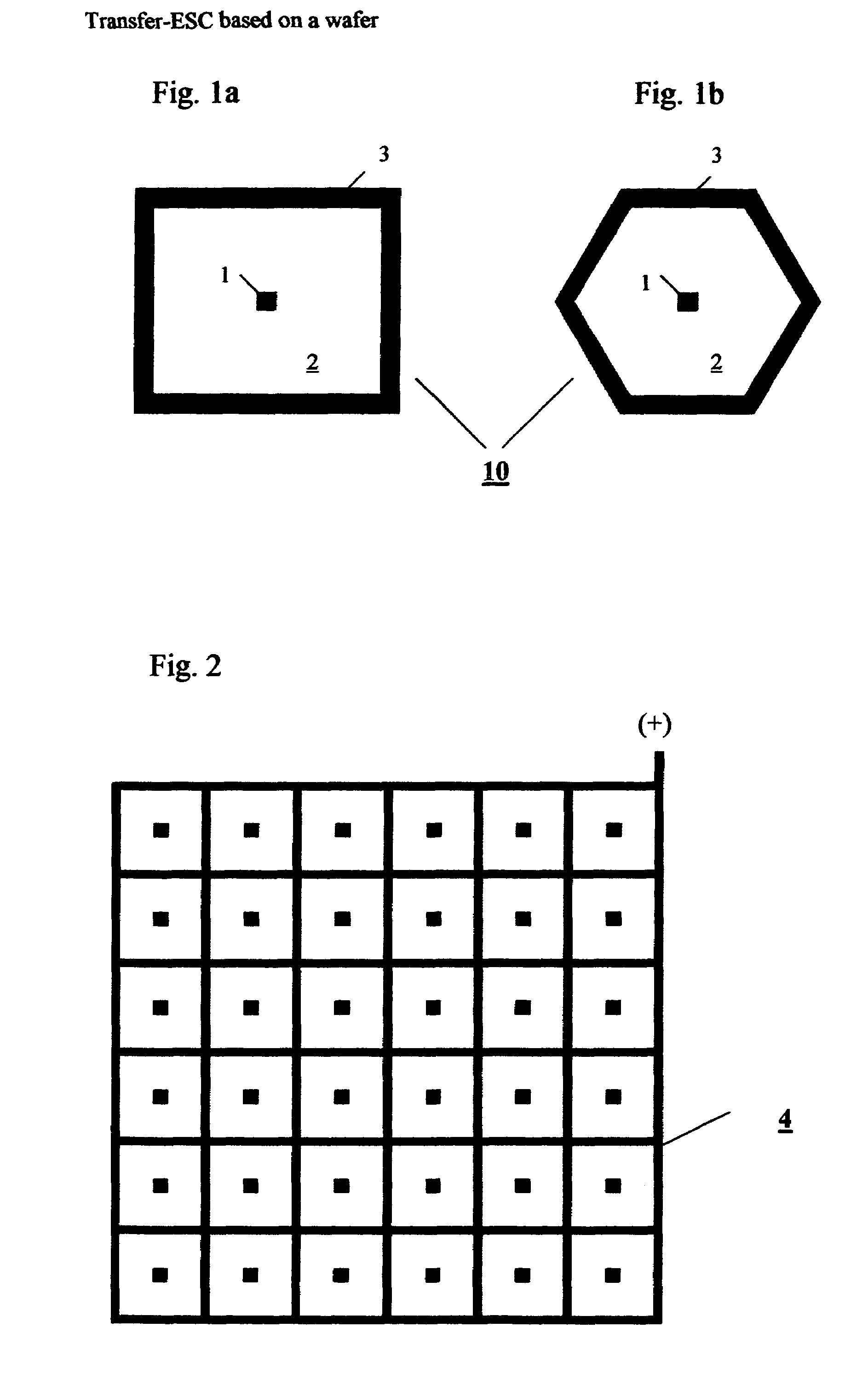
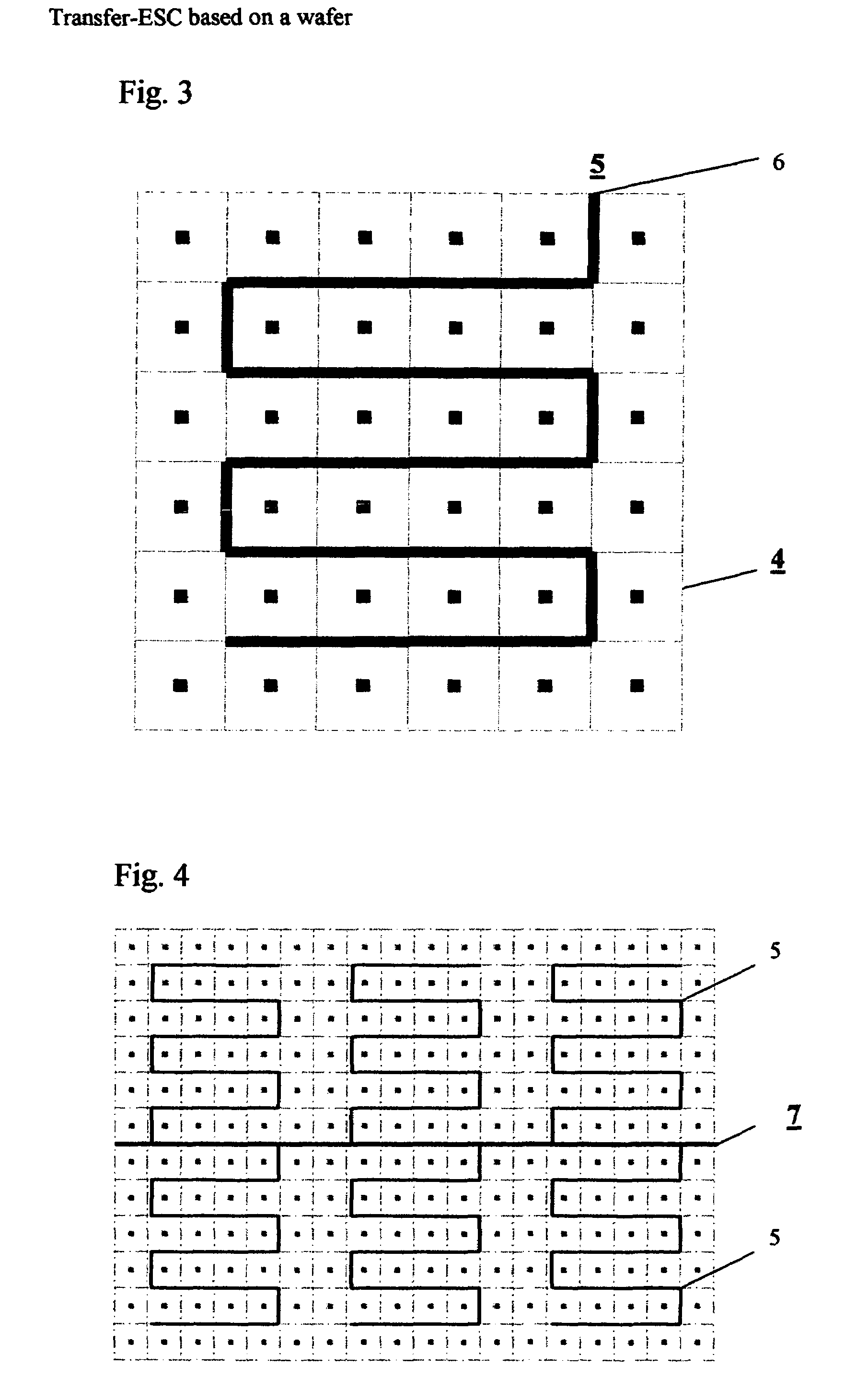
[0020]FIG. 1a shows a quadratic and FIG. 1b a hexagonal shape of an electrode-unit-cell (10). It is build up with one inside peak-electrode (1), a lateral insulator layer (2), one surrounding electrode (3) and a top dielectric layer (8). The material of choice for the inside peak-electrode (1) and the surrounding electrode (3) can be electrical conducting metals like cupper, alumina or tungsten or also highly doped poly-silicon or amorphous silicon can be employed. The used materials for the dielectric layers (2,8) are typically thermal grown-, CVD- or plasma oxides, nitrides or other suitable non conductive layers or combinations of such layers. By attaching the electrode-unit-cells (10) on each other, a complete coverage of the surface, as seen in FIG. 2, is achieved. In this case a cluster (4) of 6*6 electrode-unit-cells (10) is described.

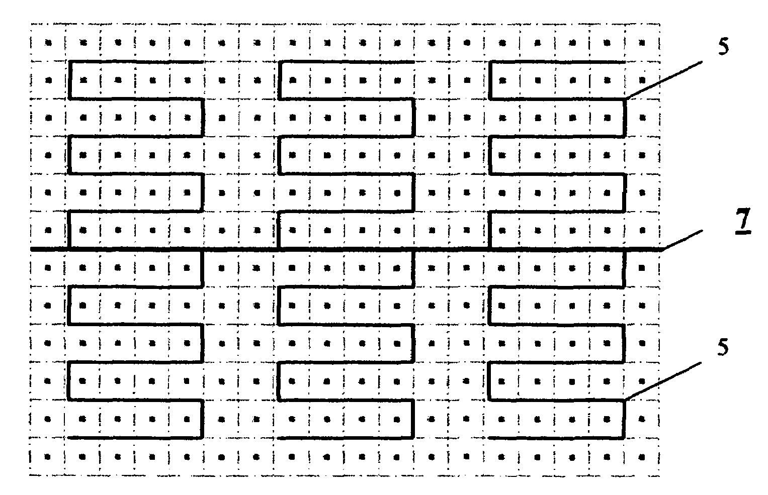
[0021]As normal for IC manufacturing technologies, many different functional levels can be allocated above each other. So an integrated fuse (5...


PUM


Abstract

A mobile transportable electrostatic chuck for clamping thin wafers (12) without permanent connection to an external power supply unit is described. The mobile chuck allows a safe handling of thin substrates on existing production equipment because the size and thickness of the clamped substrate on the mobile chuck is similar to a standard wafer. The chuck is made from silicon wafers itself as base material (11) using an IC manufacturing processes. Bipolar electrode-unit-cells (10), combined into clusters (4) and linked to an integrated fuse (5), generate a non-uniform electric field with additional force components. Peak-electrodes (1) are introduced with the highest field density in the peak region and thus creating a three dimensional non-uniform electric field with each surrounding electrode (3). Quadratic or hexagonal electrode-unit-cells (10) enable the highest dense of unit cells, which effectively clamp wafers (12) in close proximity to the surface (8a) of the chuck at elevated temperatures.

Description

FIELD OF THE INVENTION[0001]The present invention relates to an electrostatic chuck for wafers and especially to mobile, transportable electrostatic chucks (Transfer-ESC) were the mobile carrier keeps clamping a thin wafer after charging (applying a clamping voltage) without permanent connection to an external power supply unit for transportation or other process steps up to several hours.BACKGROUND OF THE INVENTION[0002]Mobile, transportable electrostatic chucks (Transfer-ESC) are used as mechanical support carriers for thin substrates. This technology is applied for the manufacturing of Integrated Circuits (IC's) within the semiconductor industry. The tendency to thinner chips or wafers is shown on RFID-Chip-products as well as for Power-Chips and many different other applications. Those support carriers allow a safe manipulating of thin, brittle wafers on existing production equipment because the size and thickness of the clamped substrate on the mobile, transportable electrostat...

Claims


Application Information

Patent Timeline
Patent Type & Authority Patents(United States)
IPC IPC(8): H02N13/00H01H23/00H01L21/68H01L21/683
CPCH01L21/6833H01L21/67709H01L21/6831H01L21/68714H01L21/68785Y10S414/141
Inventor RETZLAFF, UDO HEINZ
Owner RETZLAFF UDO HEINZ
Why Eureka
Try Eureka