Light emitting element and display device using the same

a technology of light emitting elements and display devices, applied in the direction of discharge tubes/lamp details, discharge tubes luminescnet screens, organic semiconductor devices, etc., can solve the problems of not reaching a practical level, providing sufficient reliability of elements, etc., to achieve increase the distance between the electrodes, increase the drive voltage, and reduce the resistance

Active Publication Date: 2009-08-04
SEMICON ENERGY LAB CO LTD
View PDF23 Cites 25 Cited by
  • Summary
  • Abstract
  • Description
  • Claims
  • Application Information

AI Technical Summary

Benefits of technology

[0007]It is an object of the invention to provide a highly reliable light emitting element with low drive voltage and longer life than a conventional light emitting element, and a display device using the light emitting element.
[0014]A light emitting element with little increase in resistance associated with thickening of a layer in the light emitting element can be obtained by a synergistic effect of forming the layer with a combination of an organic material and an inorganic material. Accordingly, a distance between the electrodes can be increased by forming a thick light emitting element interposed between a pair of electrodes, without increase in drive voltage. Therefore, a short circuit between the electrodes can be prevented and reliability of the light emitting element can be improved.
[0015]In addition, a highly reliable display device, which can prevent defects associated with a short circuit between the electrodes and withstand the use for a long period of time, can be obtained by applying the light emitting element obtained according to the invention to the display device.

Problems solved by technology

However, the method disclosed in Reference 1 cannot provide the element with sufficient reliability, and has not reached a practical level.

Method used


Image

  • Light emitting element and display device using the same
  • Light emitting element and display device using the same
  • Light emitting element and display device using the same

Examples


embodiment mode 1

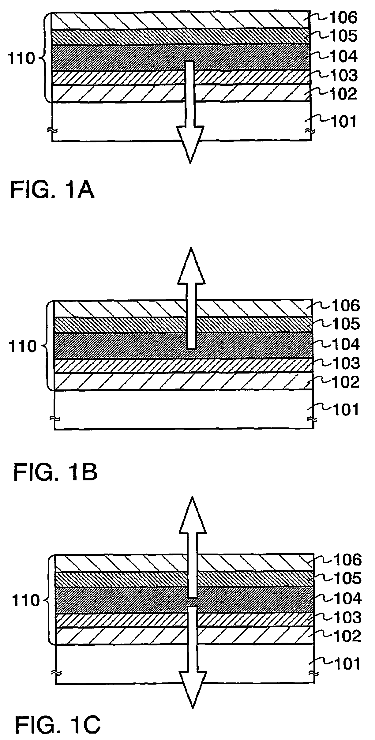
[0030]In this embodiment mode, one mode of a light emitting element is hereinafter explained with reference to FIGS. 1A to 1C.

[0031]In this embodiment mode, a light emitting element 110 is provided over a substrate 101 for supporting it, and includes a first electrode 102, a first layer 103, a second layer 104, and a third layer 105 sequentially laminated over the first electrode 102, and a second electrode 106 provided thereover (FIGS. 1A to 1C).

[0032]The substrate 101 may be a glass substrate of, for example, barium borosilicate glass, aluminoborosilicate glass, or the like, a quartz substrate, a ceramic substrate, or the like. Alternatively, a substrate made from a synthetic resin having flexibility, such as plastics, may be used. Note that a surface of the substrate 101 may be planarized in advance by polishing with a CMP method.

[0033]The first electrode 102 is preferably formed of metal, an alloy, a conductive compound, a mixture thereof, or the like, having a high work functio...

embodiment mode 2

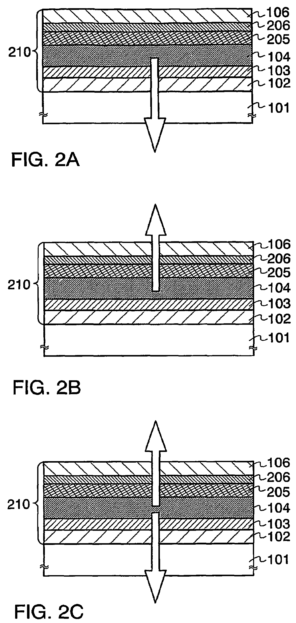
[0051]In this embodiment mode, another mode of a light emitting element, which is different from that in the above embodiment mode, is explained with reference to FIGS. 2A to 2C. Note that, in this embodiment mode, the same reference numeral is used to denote the same component as in the above embodiment mode.

[0052]In this embodiment mode, a light emitting element 210 is provided over a substrate 101 for supporting it, and it includes a first electrode 102, a first layer 103, a second layer 104, a third layer 205, and a fourth layer 206 sequentially laminated over the first electrode 102, and a second electrode 106 provided thereover (FIGS. 2A to 2C). Note that the fourth layer 206 is formed using the same material as the third layer 105 in FIGS. 1A to 1C. In other words, in this embodiment mode, a layer is newly provided between the second layer 104 and the third layer 105 in the structure of the light emitting element 110 shown in FIGS. 1A to 1C.

[0053]The third layer 205 is formed...

embodiment mode 3

[0059]In this embodiment mode, another mode of a light emitting element, which is different from those in the above embodiment modes, is explained with reference to FIGS. 3A to 3C. Note that, in this embodiment mode, the same reference numeral is used to denote the same component as in the above embodiment mode.

[0060]In this embodiment mode, a light emitting element 310 is provided over a substrate 101 for supporting it, and it includes a first electrode 102, a first layer 103, a second layer 104, a third layer 205, and a fourth layer 207 sequentially laminated over the first electrode 102, and a second electrode 106 provided thereover as shown in FIGS. 3A to 3C. In other words, the fourth layer 206 is replaced by a layer formed of a different material in the structure of the light emitting element 210 shown in FIGS. 2A to 2C.

[0061]The fourth layer 207 is formed of a layer containing both a highly electron transporting material and an electron donating material which can donate elec...


PUM


Abstract

An object of the invention is to provide a highly reliable light emitting element with low drive voltage and longer life than a conventional light emitting element, and a display device using the light emitting element. A light emitting element according to the invention comprises a plurality of layers which is interposed between a pair of electrodes, in which at least one of the plurality of layers is formed of a layer containing a light emitting material, and the layer containing a light emitting material is interposed between a layer containing an oxide semiconductor and / or metal oxide and a material having a higher hole transporting property than an electron transporting property, and a layer containing an oxide semiconductor and / or metal oxide, a material having a higher electron transporting property than a hole transporting property and a material which can donate electrons to the material having a higher electron transporting property than a hole transporting property.

Description

TECHNICAL FIELD[0001]The present invention relates to a light emitting element in which a plurality of layers is interposed between a pair of electrodes. The invention also relates to a display device using the light emitting element.BACKGROUND ART[0002]In recent years, a device utilizing light emission from an electroluminescent element (light emitting element) has attracted attention as a device for display, lighting, or the like. As the light emitting element used in such a device, well-known is a light emitting element in which a layer containing a light emitting compound is interposed between a pair of electrodes.[0003]In such a light emitting element, a hole injected from one of the electrodes is recombined with an electron injected from the other to form an excited molecule. When the excited molecule returns to a ground state, light is emitted.[0004]Meanwhile, there is a strong demand particularly for lower power consumption of a display device to be incorporated in various i...

Claims


Application Information

Patent Timeline
Patent Type & Authority Patents(United States)
IPC IPC(8): H01J1/62H01L51/50
CPCH01L51/5088H01L51/5092H01L27/3244H01L51/007H01L51/0081H01L2251/5323H01L51/5052H10K59/12H10K85/6565H10K85/324H10K50/165H10K50/17H10K50/171H10K2102/3031H05B33/14
Inventor IKEDA, HISAOSAKATA, JUNICHIROKUMAKI, DAISUKESEO, SATOSHI
Owner SEMICON ENERGY LAB CO LTD
Why Eureka
Try Eureka