Semiconductor memory device with adjustable selected work line potential under low voltage condition

a memory device and work line potential technology, applied in the field of static semiconductor memory device construction, can solve the problems of difficult compensation, complicated supply circuit, inability to stably and reliably write and read data with a low power supply voltage, etc., and achieve the effect of simple circuit construction and stable reading and writing of data

Active Publication Date: 2009-08-04
RENESAS ELECTRONICS CORP
View PDF6 Cites 52 Cited by
  • Summary
  • Abstract
  • Description
  • Claims
  • Application Information

AI Technical Summary

Benefits of technology

[0017]An object of the present invention is to provide a semiconductor memory device which allows stable reading and writing of data even with a low power supply voltage with a simple circuit construction.
[0018]Another object of the present invention is to provide a semiconductor memory device that adjusts a selected word line potential while flexibly following a threshold voltage of a memory cell transistor, and thereby can ensure write and read margins even with a low power supply voltage.

Problems solved by technology

Consequently, the semiconductor memory device cannot stably and reliably write and read data with a low power supply voltage.
Therefore, two kinds of voltages are required for the memory cell power supply voltage, which results in a problem that a power supply circuit becomes complicated for implementing the two-power-supply construction.
Therefore, even when variations occur in threshold voltage of the memory cell transistor due to fluctuations in process parameters, the switching voltage level does not change in close linkage with such variations, so that it is difficult to compensate for the changes in threshold voltage, and it is difficult to ensure reliably the write and read margins when changes occur in electric characteristics of the memory cell transistors such as threshold voltages.
In the Prior Art Reference 1, the power supply for the level shift must be arranged independently of and separately from the circuitry of the memory cell power supply, which complicates the construction of the power supply related circuitry.

Method used


Image

  • Semiconductor memory device with adjustable selected work line potential under low voltage condition
  • Semiconductor memory device with adjustable selected work line potential under low voltage condition
  • Semiconductor memory device with adjustable selected work line potential under low voltage condition

Examples


first embodiment

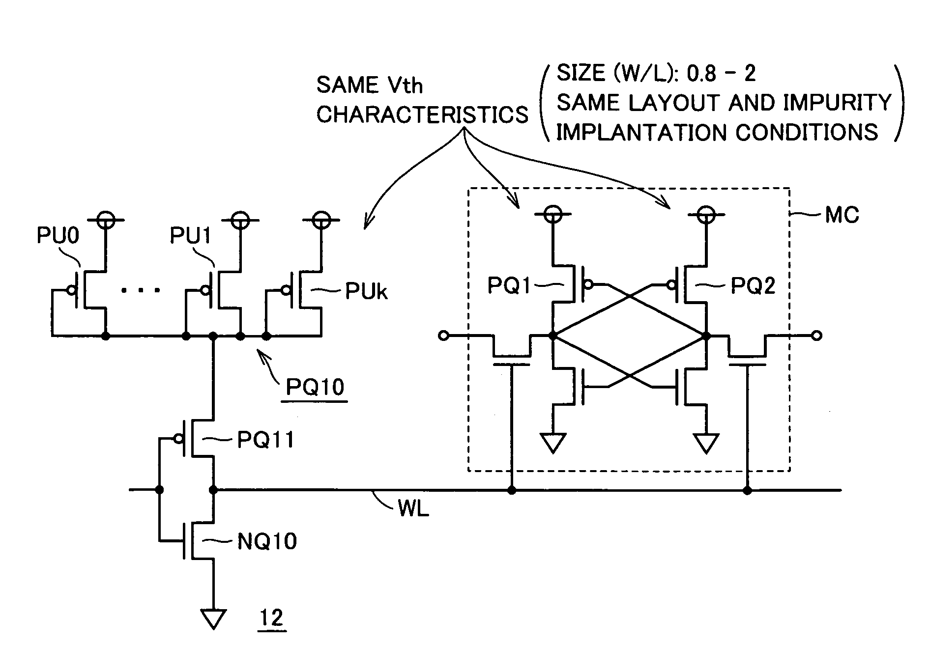
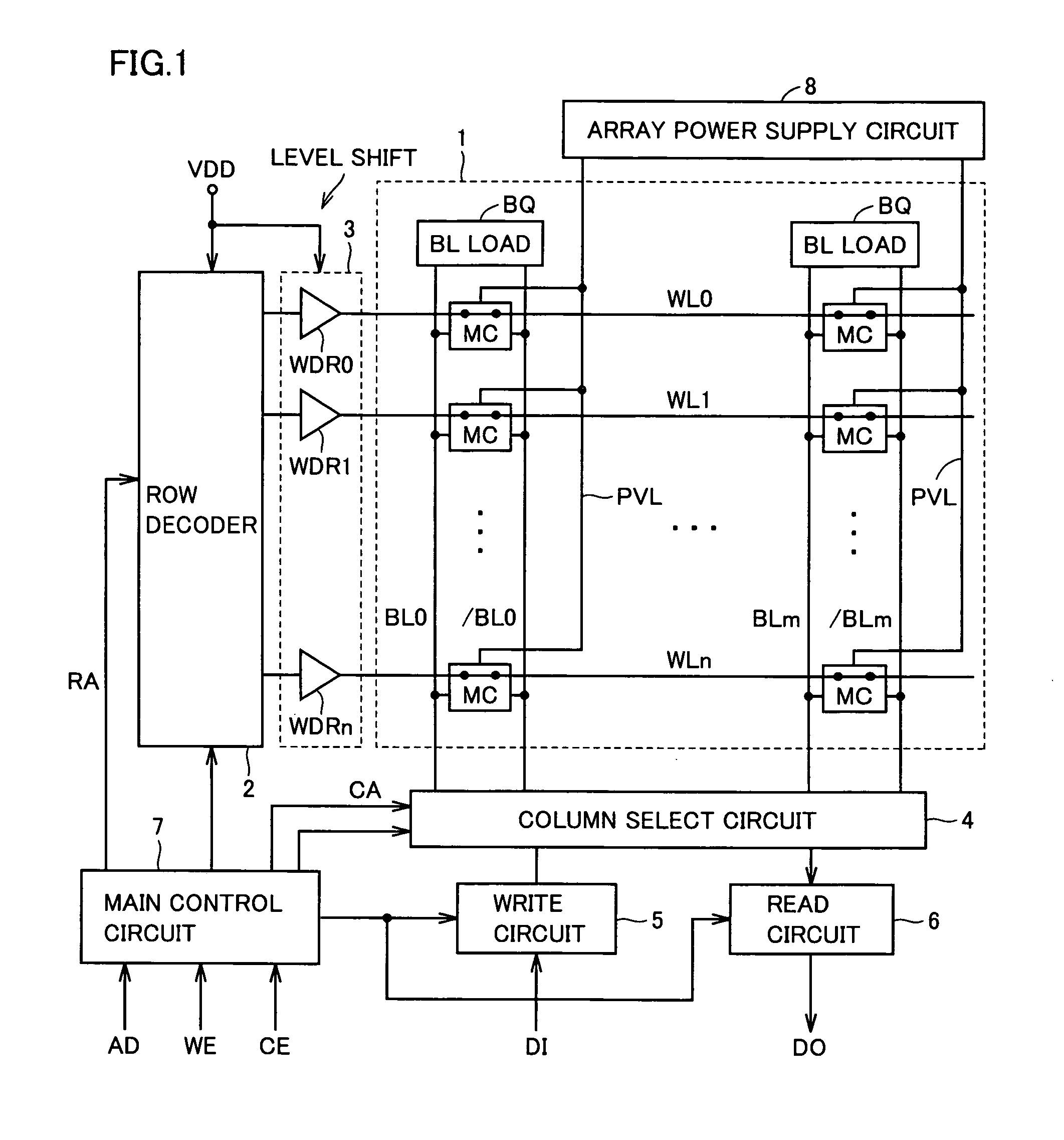
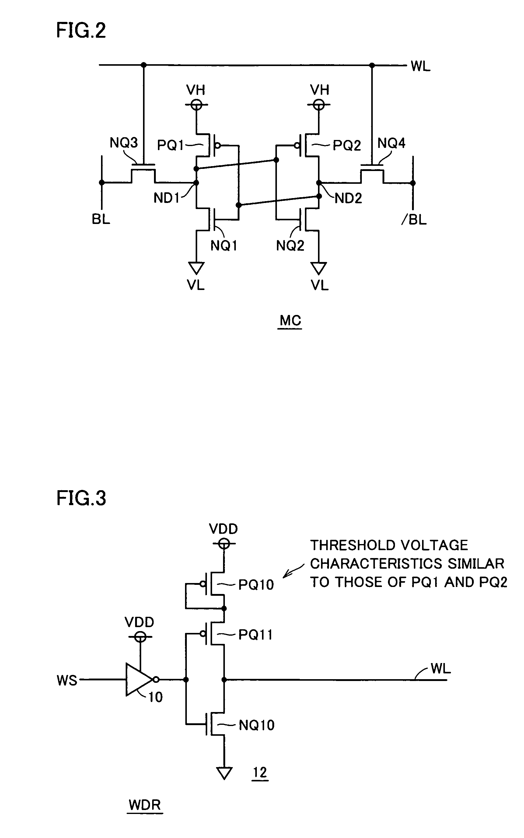
[0091]FIG. 1 schematically shows a whole construction of a semiconductor memory device according to a first embodiment of the invention. In FIG. 1, a semiconductor memory device includes a memory cell array 1 having memory cells MC arranged in rows and columns. In memory cell array 1, memory cells MC are arranged in (n+1) rows and (m+1) columns.

[0092]Word lines WL0-WLn are arranged corresponding to the rows of memory cells MC, respectively, and memory cells MC in each row are connected to the word line in the corresponding row. Bit line pairs BL0 and / BL0-BLm and / BLm are arranged corresponding to the columns of memory cells MC, respectively. As will be described later in detail, memory cell MC is a static memory cell, and complementary data are transmitted to complementary bit line pair BLi and / BLi (i=0−m).

[0093]Bit line load (BL load) BQ is provided corresponding to each of bit line pairs BL0 and / BL0-BLm and / BLm. In a data reading operation, bit line load BQ pulls up a potentia...

second embodiment

[0130]FIG. 7 schematically shows a whole construction of a semiconductor memory device according to a second embodiment of the invention. The semiconductor memory device shown in FIG. 7 differs in the following constructions from the semiconductor memory device shown in FIG. 1.

[0131]Word line drive circuit 3 includes word line drivers WDV provided corresponding to word lines WL0-WLn, respectively. Word line driver WDV does not have a level shifting function. Word line drivers WDV receive power supply voltage VDD as the operation power supply voltage, and drive a selected word line among word lines WL0-WLn to the level of power supply voltage VDD according to the word line select signal applied from row decoder 2.

[0132]Pull-down elements PD are arranged for word lines WL0-WLn, respectively. Pull-down element PD forms a resistance-dividing circuit together with a charging P-channel MOS transistor (PQ15) included in word line driver WDV and will be described later with reference to FIG...

third embodiment

[0193]FIG. 17 shows a construction of pull-down element PD according to a third embodiment of the invention. In FIG. 17, pull-down element PD includes an N-channel MOS transistor NQ25 that is connected between a word line and the ground node, and receives a complementary write instruction signal / WE at a gate thereof. Word line driver WDV has the same construction as word line driver WDV shown in FIG. 8. Corresponding portions are allotted with the same reference numerals, and description thereof is not repeated.

[0194]Main control circuit 7 shown in FIG. 7 produces a complementary write instruction signal / WE, and the whole construction of a semiconductor memory device of the third embodiment of the invention is the same as that shown in FIG. 7.

[0195]Complementary write instruction signal / WE is produced from write instruction signal WE, and attains the H and L levels in the data read mode and the data write mode, respectively.

[0196]FIG. 18 represents signal waveforms appearing on m...


PUM


Abstract

A level shift element adjusting a voltage level at the time of selection of a word line according to fluctuations in threshold voltage of a memory cell transistor is arranged for each word line. This level shift element lowers a driver power supply voltage, and transmits the level-shifted voltage onto a selected word line. The level shift element can be replaced with a pull-down element for pulling down the word line voltage according to the threshold voltage level of the memory cell transistor. In either case, the selected word line voltage level can be adjusted according to the fluctuations in threshold voltage of the memory cell transistor without using another power supply system. Thus, the power supply circuitry is not complicated, and it is possible to achieve a semiconductor memory device that can stably read and write data even with a low power supply voltage.

Description

BACKGROUND OF THE INVENTION[0001]1. Field of the Invention[0002]The present invention relates to a semiconductor memory device, and particularly to a construction of a static semiconductor memory device that can stably write and read data even under an operation condition of a low voltage.[0003]2. Description of the Background Art[0004]When transistor elements are miniaturized according to progress of miniaturization technology, voltage scaling according to the miniaturization is required from the viewpoint of reliability and power consumption of the elements. However, the miniaturization increases an influence on fluctuations in manufacturing parameters, so that a threshold voltage of transistors (insulated gate field effect transistor) forming memory cells is greatly varied, and an operation margin thereof lowers. Consequently, the semiconductor memory device cannot stably and reliably write and read data with a low power supply voltage.[0005]Various constructions have been propos...

Claims


Application Information

Patent Timeline
Patent Type & Authority Patents(United States)
IPC IPC(8): G11C7/00
CPCG11C8/08G11C11/417G11C5/14G11C5/06G11C11/413G11C11/4085G11C11/419
Inventor NII, KOJIOHBAYASHI, SHIGEKITSUKAMOTO, YASUMASAYABUUCHI, MAKOTO
Owner RENESAS ELECTRONICS CORP
Why Eureka
Try Eureka