Reduction of interference pickup in heads for magnetic recording by minimizing parasitic capacitance
a parasitic capacitance and interference pickup technology, applied in the field of magnetic storage devices, can solve problems such as adverse effects on error rate performance, and achieve the effect of reducing the capacitance of various head elements and reducing the high frequency interference pickup
- Summary
- Abstract
- Description
- Claims
- Application Information
AI Technical Summary
Benefits of technology
Problems solved by technology
Method used
Image
Examples
second embodiment
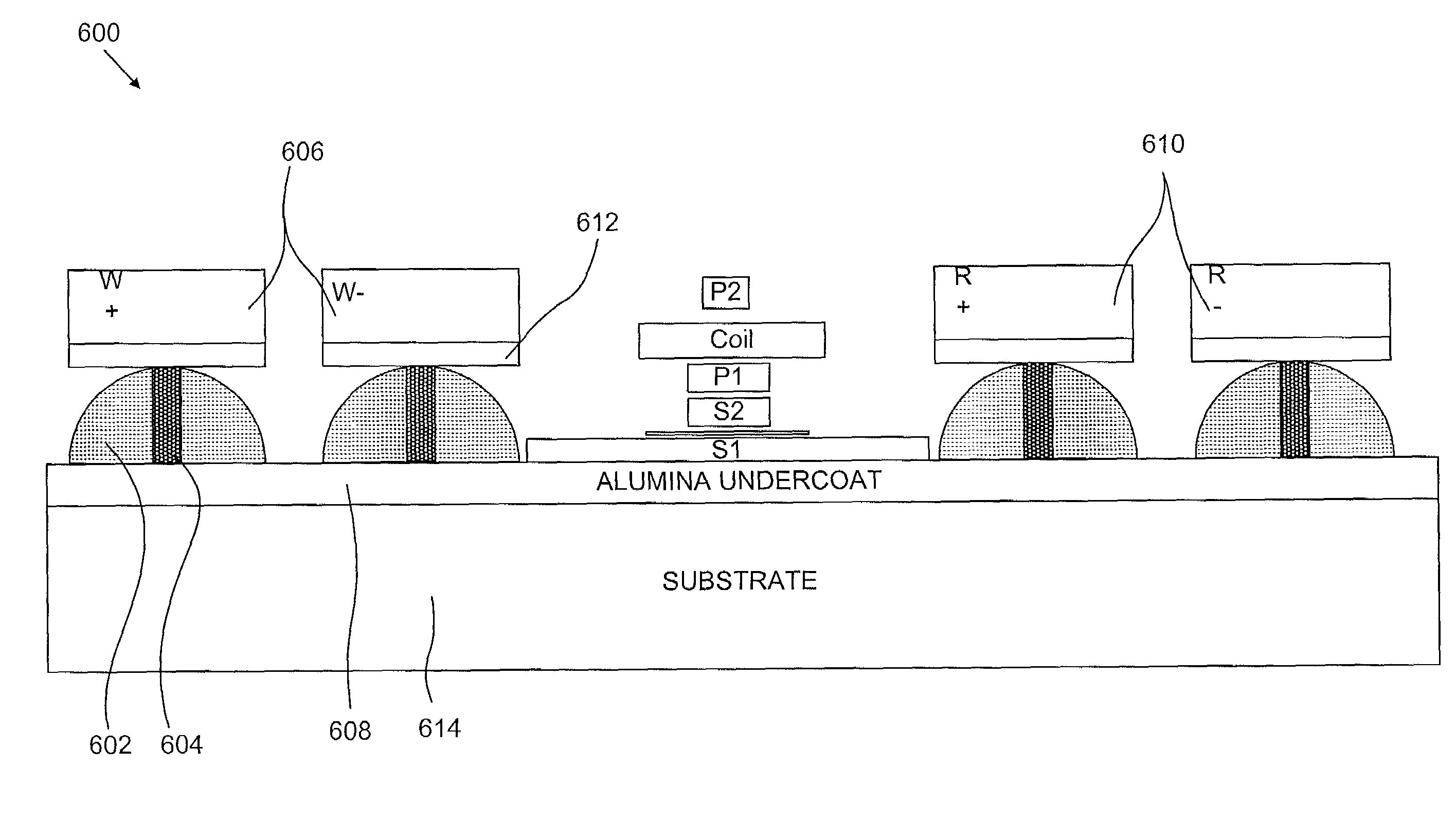
[0039]the present invention is designed to reduce high frequency interference by increasing the separation between the contact pads 610 and the substrate material 614. One example of a manner of achieving a greater separation between the contact pads 610 and the substrate material 614 is to increase the thickness of the alumina undercoat 608. The layer of alumina undercoat 608 is deposited prior to the S1 layer 314 (seen in FIG. 3). A thickness of between about 20 to about 30 microns is preferably deposited, whereas prior art thicknesses have been about 3.5 μm to about 5 μm. The alumina undercoat 608 preferably comprises Al2O3, but may also comprise silicon oxide (SiO2).
[0040]The thick layer of the alumina undercoat 608 increases the distance between the contact pads 610 and substrate material 614, which leads to a reduction in high frequency interference picked up by the read elements 610.
third embodiment
[0041]the present invention comprises suspending the contact pads 610 on studs 604 as described previously, and using a material 602 having a low dielectric constant as a spacer layer between the contact pads 610 and the substrate 614. Under this embodiment, the need to increase the thickness of the alumina undercoat 608 may be eliminated. An increase in the thickness of the alumina undercoat 608 is less preferred, as it may introduce stress in the film and create a delimitation from the substrate material 614. The low dielectric material 602 preferably has a dielectric constant less then about 10 and a more preferably dielectric constant of about 3. An example of a low dielectric material 602 placed as a spacer between the contact pads 610 and the substrate 614 comprises silicon dioxide, which has a dielectric constant of about 3. FIG. 6 depicts a hard photoresist encapsulating the studs 604 and is used as a platform for the contact pads 610. The small area of the studs 604 leads t...
PUM
| Property | Measurement | Unit |
|---|---|---|
| thickness | aaaaa | aaaaa |
| thickness | aaaaa | aaaaa |
| thickness | aaaaa | aaaaa |
Abstract
Description
Claims
Application Information


