Integration method of high-density thick-film hybrid integrated circuit without lead ball

A thick film hybrid, integrated circuit technology, applied in circuits, electrical components, electrical solid devices, etc., to achieve the effect of reducing volume, improving frequency characteristics and integration, broad market prospects and application space

Active Publication Date: 2016-05-04
GUIZHOU ZHENHUA FENGGUANG SEMICON
View PDF4 Cites 0 Cited by
  • Summary
  • Abstract
  • Description
  • Claims
  • Application Information

AI Technical Summary

Problems solved by technology

At present, there is no application for leadless ball pin surface mount high-density thick film hybrid integrated circuit

Method used


Image

  • Integration method of high-density thick-film hybrid integrated circuit without lead ball
  • Integration method of high-density thick-film hybrid integrated circuit without lead ball
  • Integration method of high-density thick-film hybrid integrated circuit without lead ball

Examples


Embodiment

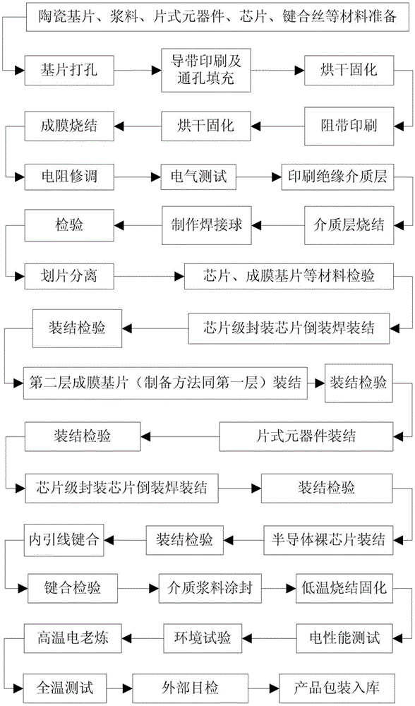
[0022] Example: The technological process of the inventive method is as Figure 11 shown, including the following steps:

[0023] (1) Preparation of ceramic substrate, gold paste, and ruthenium-based resistor paste;

[0024] (2) Cleaning and drying of substrates, cleaning and drying of shells;

[0025] (3) For the printing of thick film conduction tape paste, dry at 150°C for 10 minutes; at the same time, fill with metal paste for through holes;

[0026] (4) Printing of resistance paste, drying at 150°C for 10 minutes;

[0027] (5) Film formation and sintering at 850°C for 10 minutes, and the total film formation time is 35 minutes;

[0028] (6) Laser adjustment resistance;

[0029] (7) Parameter and function test;

[0030] (8) Print aluminum oxide ceramic insulating dielectric paste, sinter at a temperature of 650°C for 60 minutes, and sinter to form a film in a nitrogen-protected environment;

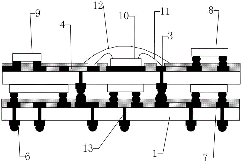
[0031] (9) Gold welding balls are formed by ignition with high-pressure g...


PUM


Abstract

The invention discloses an integration method of a surface-mounted high-density thick-film hybrid integrated circuit without lead ball pins. The method is adopted on a ceramic substrate, and the external connection end of the thick-film hybrid integrated circuit is directly made on the bottom surface of the ceramic substrate, and connected externally. The end is a metal spherical type; hybrid integration is carried out on the front of the ceramic substrate, and the thick film conduction band, thick film stop band, thick film capacitor, thick film inductor, etc. are sealed and insulated with an insulating medium thick film; the semiconductor bare chip Use insulating dielectric slurry for coating and curing protection; use three-dimensional (3D) vertical stacking method for integration to improve integration density. The characteristics of this method are: ①The volume is greatly reduced; ②The high-frequency interference is reduced; ③The length of the conduction band is reduced, and the frequency characteristics and integration are improved; ④The integration density is increased; ⑤The equipment volume is reduced, and the high-frequency performance is improved; reliability. The integrated circuit produced by the method is widely used, and is suitable for the fields of equipment miniaturization, high frequency and high reliability.

Description

technical field [0001] The present invention relates to an integrated circuit, more specifically, to a thick-film hybrid integrated circuit, especially to a surface-mounted thick-film hybrid integrated circuit. Background technique [0002] In the original hybrid circuit integration technology, on the ceramic substrate, the semiconductor chips and chip components are directly mounted on the thick film substrate, and then the bonding wire (gold wire or silicon aluminum wire) is used to bond the chip and the substrate. Wire bonding, the wire bonding of the substrate and the pins, completes the entire electrical connection, and finally seals the tube base and the tube cap in a specific atmosphere. The main problem existing in the integration technology of the original hybrid circuit is that the internal circuit must be packaged with the tube base and the tube cap. Because the tube base and the tube cap are bulky, the pins are long, and the inner leads connecting the pins are ma...

Claims


Application Information

Patent Timeline
Patent Type & Authority Patents(China)
IPC IPC(8): H01L21/48H01L21/56H01L21/98
CPCH01L24/73H01L2224/16225H01L2224/32225H01L2224/45144H01L2224/48227H01L2224/73253H01L2224/73265H01L2224/81193H01L2225/1023H01L2225/1058H01L2924/15192H01L2924/15311H01L2924/15331
Inventor 杨成刚王德成苏贵东黄晓山
Owner GUIZHOU ZHENHUA FENGGUANG SEMICON
Why Eureka
Try Eureka