Semiconductor distributed feedback (DFB) laser array with integrated attenuator

a distributed feedback and laser array technology, applied in the field of optical devices, can solve the problems of low optical absorption, achieve the effects of improving device operation, reducing power exiting the device, and increasing curren

Active Publication Date: 2009-08-11
NEOPHOTONICS CORP
View PDF37 Cites 14 Cited by
  • Summary
  • Abstract
  • Description
  • Claims
  • Application Information

AI Technical Summary

Benefits of technology

[0015]In some embodiments, an array of such attenuators is fabricated at the output of a laser array. The attenuating devices are all be shorted together and controlled with a single contact, in further embodiments. Device operation can be improved somewhat, particularly when an array geometry is used by applying a small forward bias to help obtain transparency, and a reverse bias to collect the photogenerated carriers.
[0016]For example, an integrated optoelectronic chip where the output power can be controlled without degrading other optical characteristics comprises a laser section that generates light and contains gratings for providing feedback, an attenuator section that contains active material (such as quantum wells) but no gratings, and external means of adjusting the attenuator to reduce the power exiting the device.
[0017]In some embodiments the active material in the attenuator has the same composition as the active material in the laser. The external means collects photocurrent from the integrated optoelectronic chip, increased current leading to increased attenuation. The multiple lasers and multiple attenuators may be fabricated on the same chip and multiple attenuators may be connected together and accessed with a single contact pad.
[0018]The output power of an integrated optoelectronic chip can be controlled without degrading other optical characteristics. Such an integrated optoelectronic chip may comprise a laser section that generates light and contains gratings for providing feedback, an attenuator section that contains active material (such as quantum wells) but no gratings, external means of adjusting the attenuator to reduce the power exiting the device.

Problems solved by technology

However, as the input intensity increases, the absorption is quickly saturated and the section becomes largely transparent, with an insertion loss generally less than 1 dB.
The high carrier density leads to low optical absorption.

Method used


Image

  • Semiconductor distributed feedback (DFB) laser array with integrated attenuator
  • Semiconductor distributed feedback (DFB) laser array with integrated attenuator
  • Semiconductor distributed feedback (DFB) laser array with integrated attenuator

Examples


Embodiment Construction

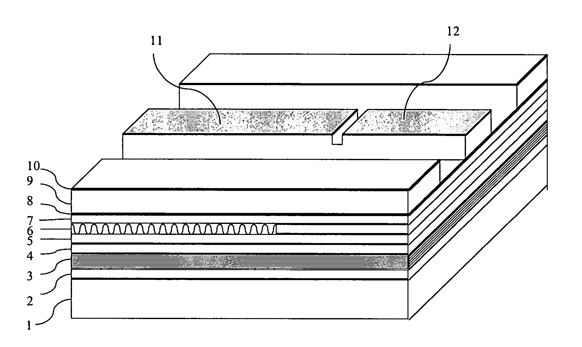
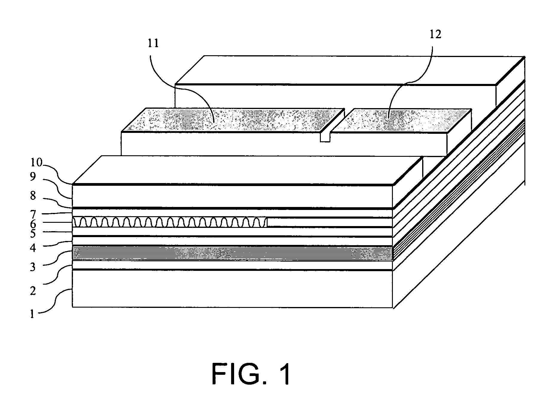
[0030]In one embodiment, a DFB laser containing gain material and a grating for feedback is integrated with a semiconductor attenuator region with an active material but no grating layer. The light from the DFB laser passes through the attenuator region. The attenuator region acts to absorb light and generates a photocurrent. If a contact to the attenuator is left open, the optical energy saturates the gain material, rendering it transparent, and the majority of the light entering from the DFB laser is transmitted out of the attenuator region. On the other hand, if the generated photocurrent is allowed to flow out of the attenuator region, the photo-generated carriers do not build up and the material continues to absorb light. Thus by adjusting the bias conditions to the attenuator region, the light intensity exiting the device can be controlled. In some embodiments, an array of lasers and attenuators is fabricated, where each laser is individually contacted, but all the attenuators...


PUM


Abstract

A semiconductor laser with an integrated attenuator on the same chip as the laser. In some embodiments the attenuator is formed of the same material as the laser, but without a grating in the attenuator. In some embodiments the laser and attenuator are fabricated concurrently, with the attenuator positioned at the front of the laser and differing from the laser only in not having a grating and having a much smaller length. Level of attenuation by the attenuator is adjustable based on drawing photogenerated current from the attenuator.

Description

CROSS-REFERENCE TO RELATED APPLICATION[0001]This application claims the benefit of the filing date of U.S. Provisional Patent Application No. 60 / 500,389, filed Sep. 5, 2003, the disclosure of which is incorporated by reference herein.BACKGROUND OF THE INVENTION[0002]This invention relates generally to optical devices, and more particularly to semiconductor laser devices.[0003]Semiconductor lasers are used for generating light that carries data in fiber-optic systems. A common form of laser for long distance fiber optic communication is a distributed feedback (DFB) laser. In a DFB a diffraction grating is embedded in the laser and controls the wavelength. These devices can be made single mode and have narrow linewidths and excellent low noise characteristics appropriate for fiber optic applications.[0004]Frequently, the intensity level from DFB lasers may require adjustment. This can occur for many reasons. For example, in wavelength division multiplexed (WDM) links, where light of m...

Claims


Application Information

Patent Timeline
Patent Type & Authority Patents(United States)
IPC IPC(8): H01S5/00H01S5/12
CPCH01S5/0265H01S5/0601H01S5/12H01S5/1039H01S5/0683
Inventor PEZESHKI, BARDIA
Owner NEOPHOTONICS CORP
Why Eureka
Try Eureka