Ballistic deflection transistor and logic circuits based on same

a transistor and ballistic deflection technology, applied in the field of transistors, can solve the problems of limiting the frequency of capacitors, requiring cooling, and less useful at room temperature, and achieve the effects of reducing power consumption, reducing noise, and reducing power consumption

Inactive Publication Date: 2009-08-18
UNIVERSITY OF ROCHESTER
View PDF4 Cites 25 Cited by
  • Summary
  • Abstract
  • Description
  • Claims
  • Application Information

AI Technical Summary

Benefits of technology

[0013]It is still another object of the invention to do so with reduced noise and reduced power consumption.
[0014]To achieve the above and other objects, the present invention utilizes a non-linearity observed in ballistic rectifiers, which is based upon the ballistic electron effect, where device feature size is small in relation to the mean free path of electrons. The net effect is that electrons behave in a semi-classical way under these conditions, and deflective structures can be used to alter the current-voltage characteristic. Fields can be used to control the path of the electrons in such a structure. By placing capacitive structures in proximity of the rectifying structure, one could alter the path of the electrons and thus where the electrons would hit the deflective structure. If one biases a current so that electrons would have a preferred path towards the deflector, such that small changes in path would result in large changes in deflection angle, an applied field to a capacitive structure can be used to select the path of those electrons. By utilizing these effects and creating a structure that can control the path of the electrons, forms a new transistor device.
[0015]This invention combines the above-noted non-linearity which is based upon ballistic electron effects whereby small deflective structures can be used to alter the current-voltage characteristic, and an electron field effect whereby electron path can be altered by the application of a small electric field to create a transistor device. This is achieved in one embodiment where deflective structure(s) input and output conductive path(s) are created in a 2D heterostructure based electron gas. Alongside or near the conductive paths or alongside or near the deflective structure, capacitive or inductive structures are created to enable the alteration of the electron path. By using electric or magnetic fields to guide the electrons to a deflective structure, the electron path can be selected to one or multiple output paths. In at least one embodiment, capacitive structures are used to alter the path of the electrons, which are sourced from the bottom of the figure towards the top. Applying either a positive or a negative electric field will alter the current path to the left or to the right port of the device. If no field is applied, the electron path will be deflected equally to the left and to the right. This structure can be further modified such that there are more than 2 output ports, and the deflective geometry can be altered such that there are multiple deflection points, which may enhance functionality. The deflector may be composed of multiple structures to create a desired deflective or transmissive effect. In addition both inductive and capacitive structures can be used and located elsewhere in the structure without loss of functionality.
[0017]The shape of the ports can be of any geometry such that it makes them suitable for the reception of electrons. A minimum size of the opening of the port is required such that electrons may enter into the port. The port is preferably designed to accommodate the geometry of the deflector and to enhance the deflector effect.

Problems solved by technology

However, these devices all suffer at least one of the following disadvantages: (1) The use of a junction that creates temperature sensitive operation, (2) the junction capacitance limits frequency of operation, (3) long electron transit times, (4) the requirement of multiple precision fabrication steps, (5) the requirement of cooling to temperatures below 300K.
It is less useful, however, at room temperature.
One reason is practical, that the electron mean free path determined by phonon scattering becomes smaller, to at most several hundred nm in any material at room temperature, so the ballistic regime is more difficult to reach.
A third reason is that the thermal energy at room temperature, kT=26 meV, is larger than the typical energy spacing of the transverse confinement modes, so it is not possible to observe any effects which require energy level quantization.
However, such effects have not been applied to address the above-noted problems of known terahertz transistors.

Method used


Image

  • Ballistic deflection transistor and logic circuits based on same
  • Ballistic deflection transistor and logic circuits based on same
  • Ballistic deflection transistor and logic circuits based on same

Examples


Embodiment Construction

[0041]Preferred embodiments of the present invention will now be set forth in detail with reference to the drawings, in which like reference numerals refer to like elements throughout.

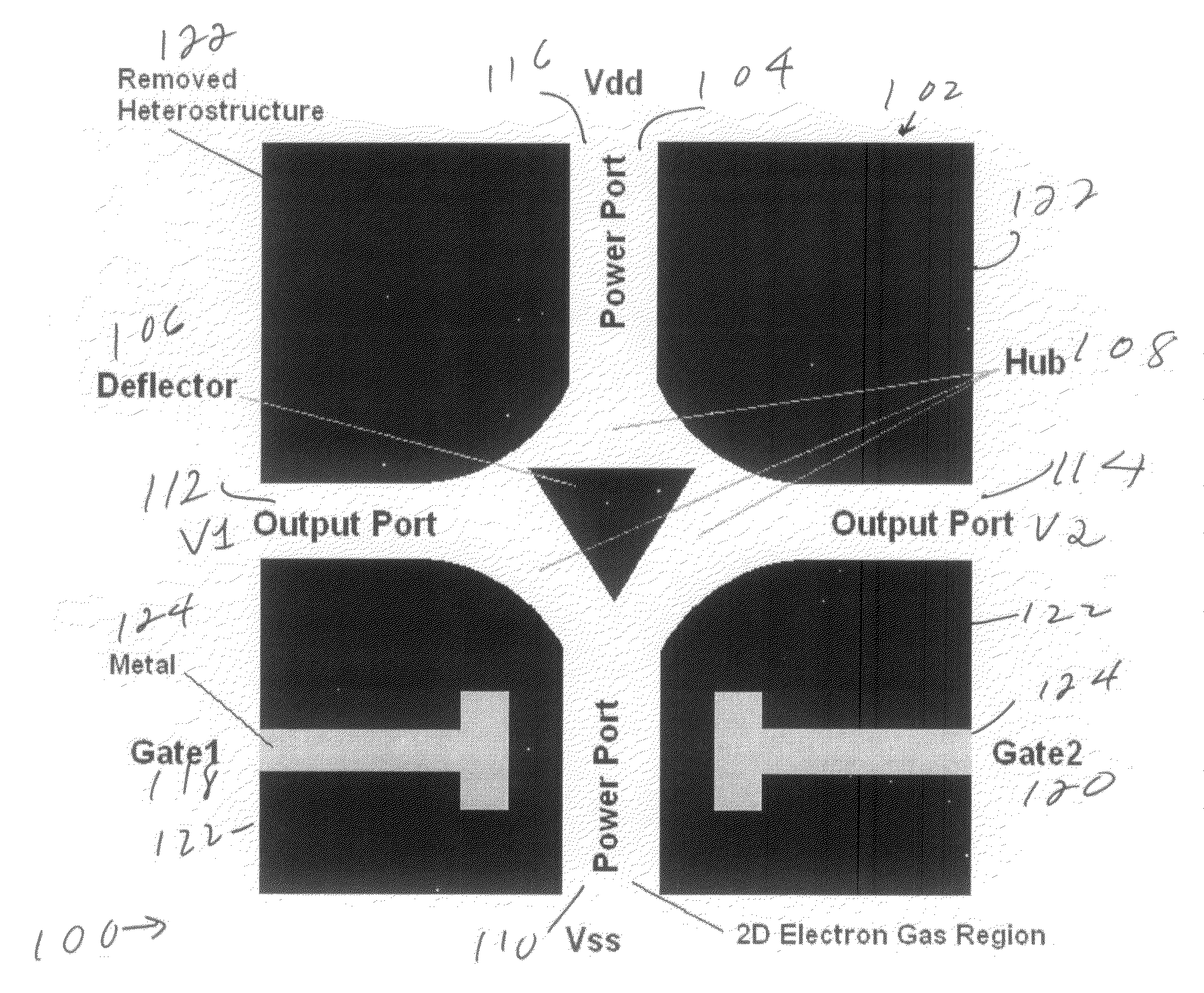
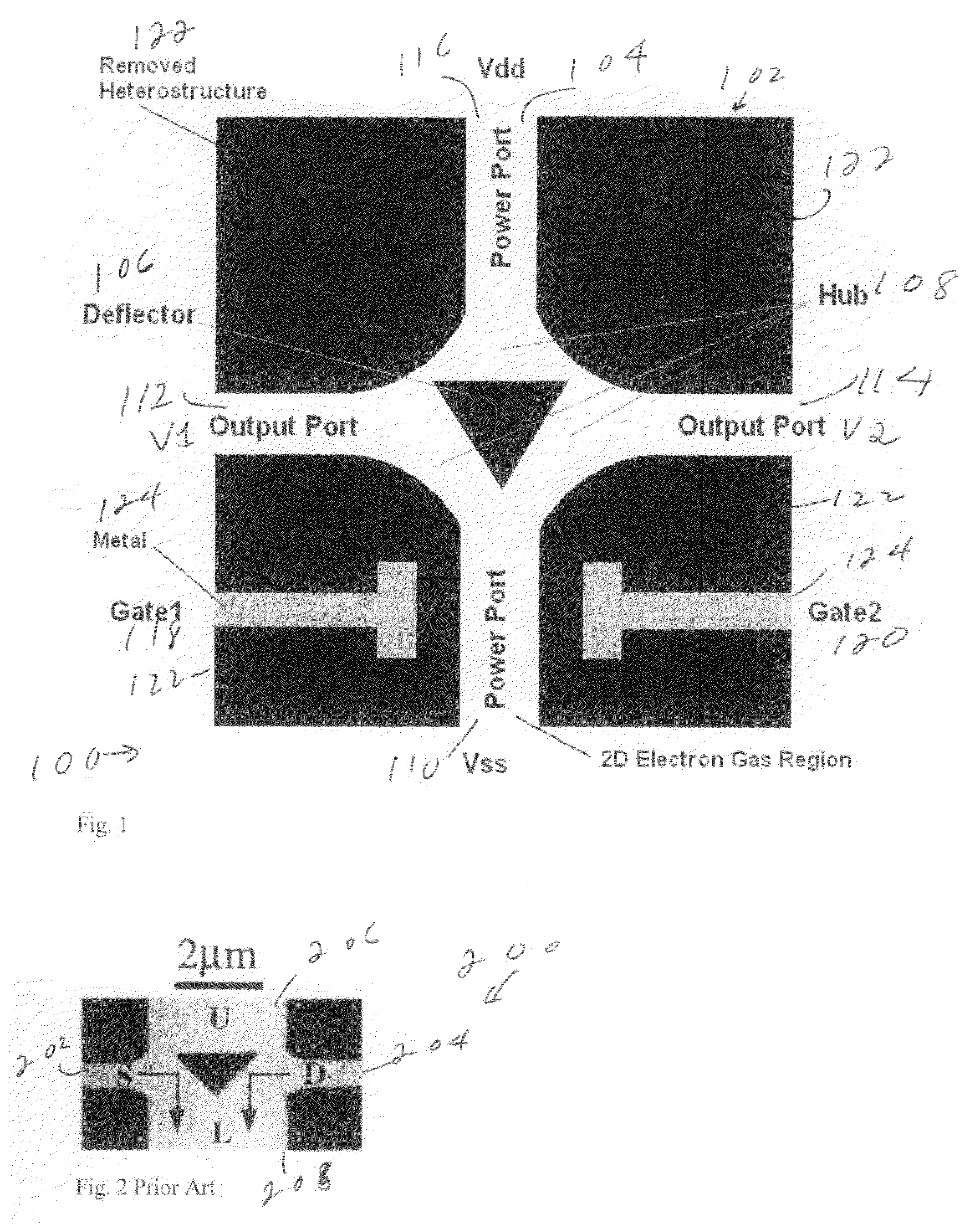
[0042]A preferred embodiment of the invention is shown in FIG. 1, where a transistor 100 is fabricated by etching a structure of given width and height and thickness into an InP substrate 102 and doping the structure such that a quantum well 104 composed of InGaAs—InP or InGaAs—AlGaAs enables the formation of the deflective structure 106, hub 108 and ports 110, 112, 114, 116. Gates 118, 120 are preferably formed by the application of two parallel strips of conductive material near the Vss port 110, preferably near the hub 108, in parallel to the Vss port 110. Another way to form the gates 118, 120 is by isolating semiconductor by an etch so as to isolate the gate regions from the channel regions. The ports and gates have conductive contacts, such as metal contacts, that connect the transistor to power ...


PUM


Abstract

A quantum well is formed in a substrate to define a hub, ports extending from the hub, and a deflective structure in the hub. Electrons move through the hub and ports according to the ballistic electron effect. Gates control the movement of the electrons, causing them to be incident on the deflective structure on one side or the other, thus controlling the direction in which they are deflected and the port through which they pass.

Description

REFERENCE TO RELATED APPLICATIONS[0001]The present application claims the benefit of U.S. Provisional Patent Application No. 60 / 832,597, filed Jul. 24, 2006, which in turn builds on concepts originally disclosed in U.S. Provisional Patent Application No. 60 / 580,374, filed Jun. 18, 2004. The disclosures of both of those applications are hereby incorporated by reference in their entireties into the present application.STATEMENT OF GOVERNMENT INTEREST[0002]The work leading to the present invention was supported in part by the Office of Naval Research, Grant No. N000140510052. The government has certain rights in the invention.FIELD OF THE INVENTION[0003]The present invention is directed to a transistor and more specifically to a transistor based on the geometrical deflection of ballistic current. The invention is further directed to logic circuits using such a transistor.DESCRIPTION OF RELATED ART[0004]Several different techniques have been attempted to increase the operating speed of ...

Claims


Application Information

Patent Timeline
Patent Type & Authority Patents(United States)
IPC IPC(8): H03K19/00H01L21/334H01L29/12
CPCB82Y10/00H01L27/0605H01L29/125H03K19/08H01L29/66977H01L29/7784H01L29/8725H01L29/205
Inventor DIDUCK, QUENTINMARGALA, MARTIN
Owner UNIVERSITY OF ROCHESTER
Why Eureka
Try Eureka