Ferroelectric memory device
a memory device and ferroelectric technology, applied in the field of semiconductor devices, can solve problems such as the inability to induce the desired spontaneous polarization
- Summary
- Abstract
- Description
- Claims
- Application Information
AI Technical Summary
Benefits of technology
Problems solved by technology
Method used
Image
Examples
first embodiment
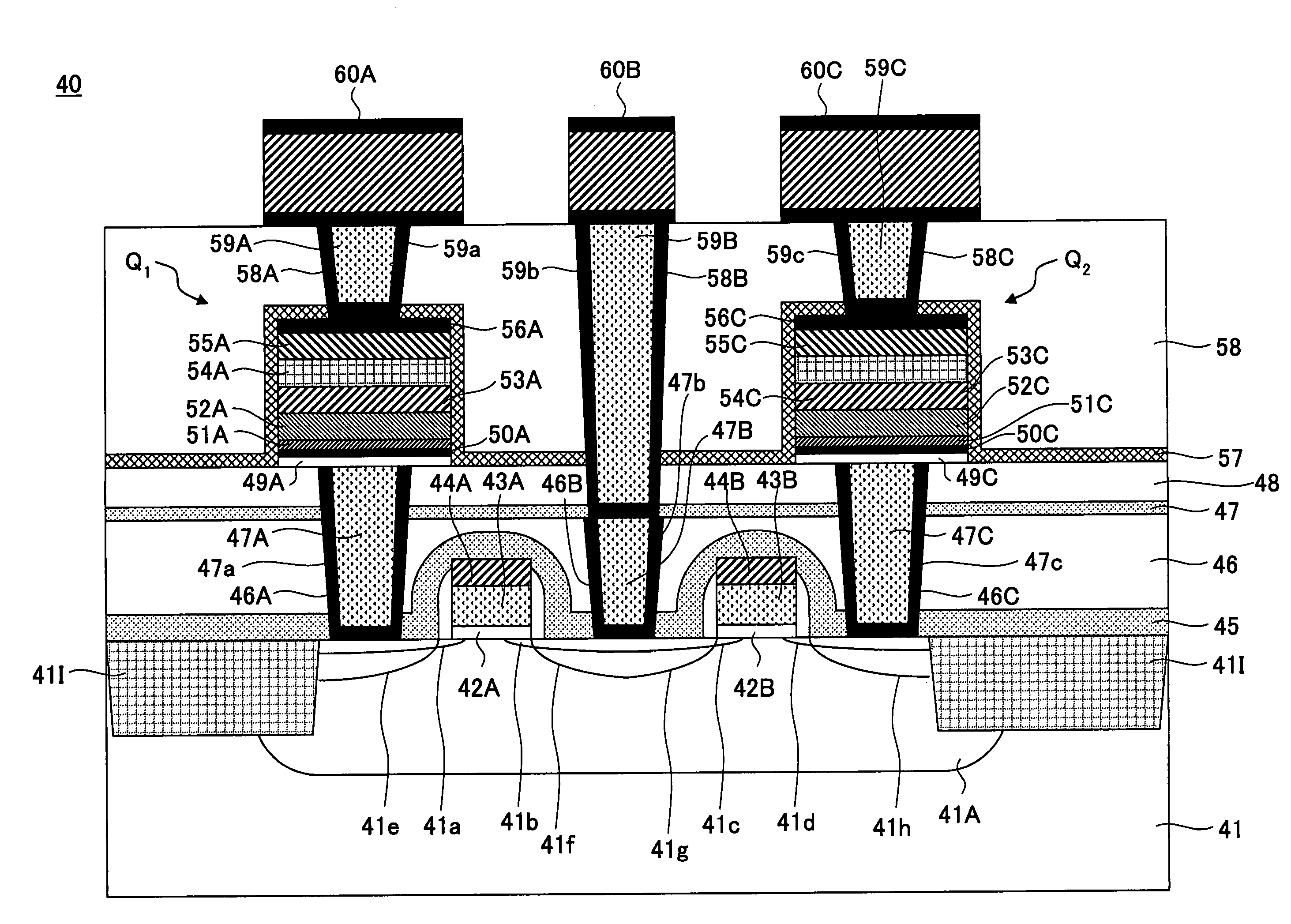
[0069]FIG. 5 shows the construction of a ferroelectric memory 40 according to a first embodiment of the present invention.
[0070]Referring to FIG. 5, the ferroelectric memory device 40 is a so-called 1T1 C type device and includes two memory cell transistors formed in a device region 41A defined on a silicon substrate 41 by a device isolation region 41I of STI (shallow trench isolation) type, so as to share a bit line.
[0071]More specifically, there is formed an n-type well in the silicon substrate 41 as the device region 41A, wherein there are formed a first MOS transistor having a polysilicon gate electrode 43A and a second MOS transistor having a polysilicon gate electrode 43B on the device region 41A respectively via a gate insulation film 42A and a gate insulation film 42B.
[0072]In the silicon substrate 41, there are formed LDD regions 41a and 41b of p−-type in correspondence to respective sidewalls of the gate electrode 43A, and there are further formed LDD regions 41c and 41d o...
second embodiment
[0147]FIG. 17 shows the construction of a ferroelectric memory device 60 according to a second embodiment of the present invention, wherein those parts of FIG. 17 corresponding to those parts explained previously are designated with the same reference numerals and the description thereof will be omitted.
[0148]Referring to FIG. 17, the ferroelectric memory device 60 has a construction similar to the ferroelectric memory device 40 explained with reference to FIG. 5, except that there are formed ferroelectric capacitors Q11 and Q12 that use PZT films 64A and 64C formed by a sputtering process.
[0149]With this, the lower electrode is formed in the ferroelectric capacitor Q11 by lamination of an Ir film 62A1 having the thickness of 100 nm, an IrOx film 62A2 having the thickness of 20 nm, a PtOx film 62A3 having the thickness of 20 nm and a Pt film 62A4 having the thickness of 100 nm.
[0150]Similarly, the lower electrode is formed in the ferroelectric capacitor Q12 by lamination of an Ir fi...
PUM
 Abstract
Description
Claims
Application Information


