Ferroelectric memory device and fabrication process thereof, fabrication process of a semiconductor device

a technology of ferroelectric memory and fabrication process, which is applied in the direction of digital storage, capacitors, instruments, etc., can solve the problem of not being able to induce the desired spontaneous polarization

Inactive Publication Date: 2007-03-01
FUJITSU SEMICON MEMORY SOLUTION LTD
View PDF10 Cites 21 Cited by
  • Summary
  • Abstract
  • Description
  • Claims
  • Application Information

AI Technical Summary

Benefits of technology

[0031] a field effect transistor formed on said semiconductor substrate, said field effect transistor including first and second diffusion regions;
[0032] an interlayer insulation film formed on said semiconductor substrate so as to cover said field effect transistor;

Problems solved by technology

Contrary to this, when the c-axis has aligned in an in-plane direction of the capacitor insulation film (100 orientation), it is not possible to induce the desired spontaneous polarization even when a drive voltage is applied to the capacitor.

Method used


Image

  • Ferroelectric memory device and fabrication process thereof, fabrication process of a semiconductor device
  • Ferroelectric memory device and fabrication process thereof, fabrication process of a semiconductor device
  • Ferroelectric memory device and fabrication process thereof, fabrication process of a semiconductor device

Examples


first embodiment

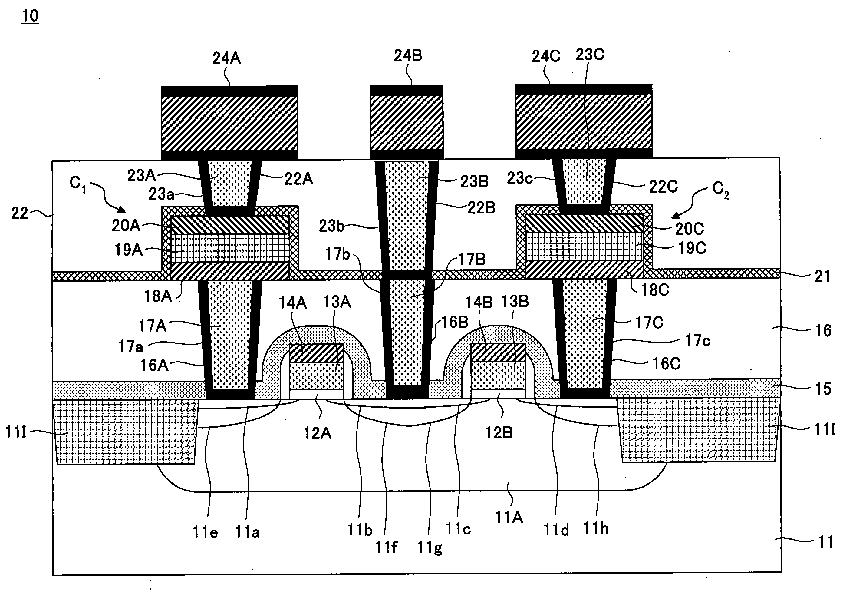
[0069]FIG. 5 shows the construction of a ferroelectric memory 40 according to a first embodiment of the present invention.

[0070] Referring to FIG. 5, the ferroelectric memory device 40 is a so-called 1T1 C type device and includes two memory cell transistors formed in a device region 41A defined on a silicon substrate 41 by a device isolation region 41I of STI (shallow trench isolation) type, so as to share a bit line.

[0071] More specifically, there is formed an n-type well in the silicon substrate 41 as the device region 41A, wherein there are formed a first MOS transistor having a polysilicon gate electrode 43A and a second MOS transistor having a polysilicon gate electrode 43B on the device region 41A respectively via a gate insulation film 42A and a gate insulation film 42B.

[0072] In the silicon substrate 41, there are formed LDD regions 41a and 41b of p−-type in correspondence to respective sidewalls of the gate electrode 43A, and there are further formed LDD regions 41c and...

second embodiment

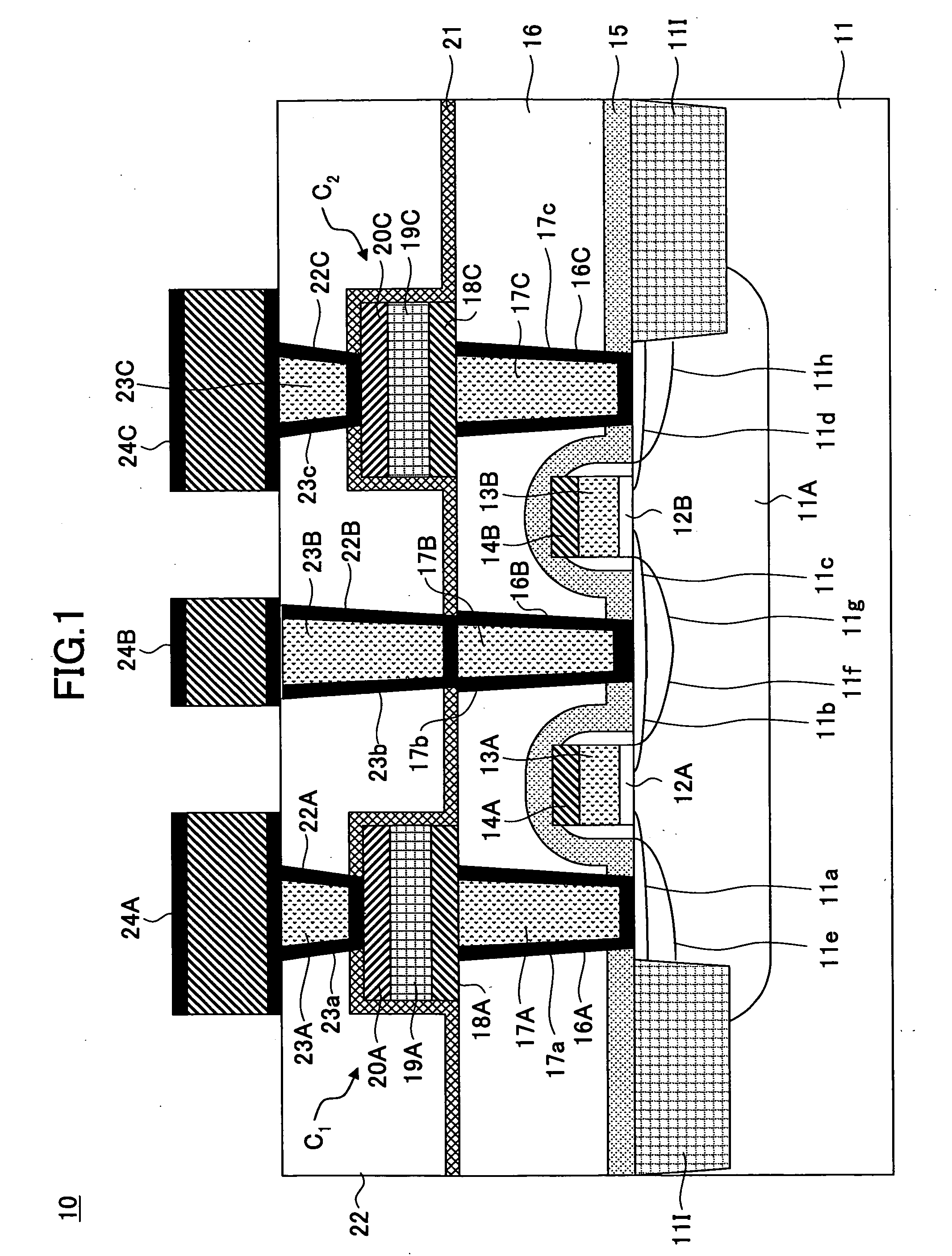
[0147]FIG. 17 shows the construction of a ferroelectric memory device 60 according to a second embodiment of the present invention, wherein those parts of FIG. 17 corresponding to those parts explained previously are designated with the same reference numerals and the description thereof will be omitted.

[0148] Referring to FIG. 17, the ferroelectric memory device 60 has a construction similar to the ferroelectric memory device 40 explained with reference to FIG. 5, except that there are formed ferroelectric capacitors Q11 and Q12 that use PZT films 64A and 64C formed by a sputtering process.

[0149] With this, the lower electrode is formed in the ferroelectric capacitor Q11 by lamination of an Ir film 62A1 having the thickness of 100 nm, an IrOx film 62A2 having the thickness of 20 nm, a PtOx film 62A3 having the thickness of 20 nm and a Pt film 62A4 having the thickness of 100 nm.

[0150] Similarly, the lower electrode is formed in the ferroelectric capacitor Q12 by lamination of an...


PUM


Abstract

A ferroelectric memory device includes a field effect transistor formed on a semiconductor substrate, an interlayer insulation film formed on the semiconductor substrate so as to cover the field effect transistor, a conductive plug formed in the interlayer insulation film in contact with the first diffusion region, and a ferroelectric capacitor formed over the interlayer insulation in contact with the conductive plug, wherein the ferroelectric capacitor includes a ferroelectric film and upper and lower electrodes sandwiching the ferroelectric film respectively from above and below, the lower electrode being connected electrically to the conductive plug, a layer containing oxygen being interposed between the conductive plug and the lower electrode, a layer containing nitrogen being interposed between the layer containing oxygen and the lower electrode, a self-aligned layer being interposed between the layer containing nitrogen and the lower electrode.

Description

CROSS-REFERENCE TO RELATED APPLICATION [0001] The present application is based on Japanese priority application No. 2005-253909 filed on Sep. 1, 2005, the entire contents of which are hereby incorporated by reference. BACKGROUND OF THE INVENTION [0002] The present invention generally relates to semiconductor devices and more particularly to a semiconductor device having a ferroelectric capacitor and fabrication process thereof. [0003] A ferroelectric memory is a non-volatile voltage-driven semiconductor memory device and is characterized by preferable feature of high operational speed, low electric power consumption and non-volatility of information in that the information held therein is retained even when the electric power is turned off. Ferroelectric memories are already used in IC cards and other portable electronic apparatuses. REFERENCES [0004] Patent Reference 1 the Japanese Laid-Open Patent Application 2004-153031 official gazette [0005]FIG. 1 is a cross-sectional diagram s...

Claims


Application Information

Patent Timeline
Patent Type & Authority Applications(United States)
IPC IPC(8): H01L29/94
CPCG11C11/22H01L27/11502H01L28/65H01L28/57H01L27/11507H10B53/30H10B53/00H01L27/105
Inventor SASHIDA, NAOYA
Owner FUJITSU SEMICON MEMORY SOLUTION LTD
Why Eureka
Try Eureka