Magnetophoretic and electromagnetophoretic displays

a technology of electromagnetophoretic display and magnetophoretic display, which is applied in the direction of identification means, instruments, writing boards, etc., can solve the problems of high large cost of transparent conductor film, and economic disadvantage, and achieves high contrast ratio, flexible and durable, and wide viewing angle

Inactive Publication Date: 2009-08-25
E INK CALIFORNIA
View PDF45 Cites 45 Cited by
  • Summary
  • Abstract
  • Description
  • Claims
  • Application Information

AI Technical Summary

Benefits of technology

[0014]Similar to conventional electrophoretic displays (EPDs or EPIDs), the electromagnetophoretic displays (EMPDs) of this invention are bistable and have a very wide viewing angle. Many different driving mechanisms and circuitry designs may be employed to achieve optimum performance of the displays of this invention. Most of them do not require the use of a transparent conductor film, such as ITO film, which is expensive, fragile and often transmits or reflects less than 90% of the incipient visible light. As a result, the displays of the invention are much more flexible and durable than conventional displays and provide images of a high contrast ratio, wide viewing angle and high reflectance in the Dmin area. Furthermore, the present invention provides a great number of alternatives in design, and a particular type of design within the scope of the invention may be easily constructed to meet the needs for a variety of applications.

Problems solved by technology

However, the use of a transparent conductor film, such as indium tin oxide (ITO) on the viewing side, particularly a transparent patterned conductor film, in such large displays is an economic disadvantage as the transparent conductor film is expensive.
The expense for the transparent conductor film often is a major part of the total manufacturing cost of the electrophoretic displays.
In addition, the ITO film is brittle and only provides about 80-90% of transmission or reflection in the visible light region.

Method used


Image

  • Magnetophoretic and electromagnetophoretic displays
  • Magnetophoretic and electromagnetophoretic displays
  • Magnetophoretic and electromagnetophoretic displays

Examples


Embodiment Construction

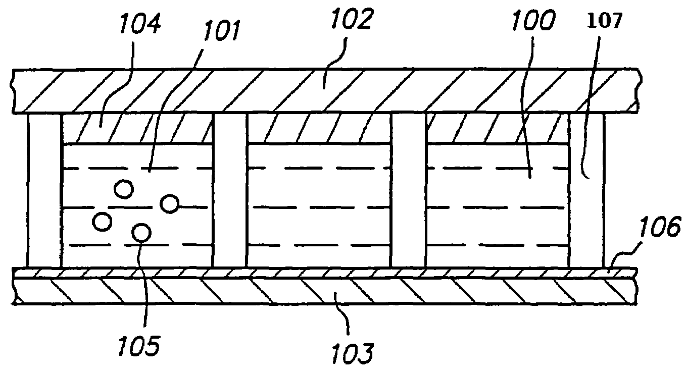
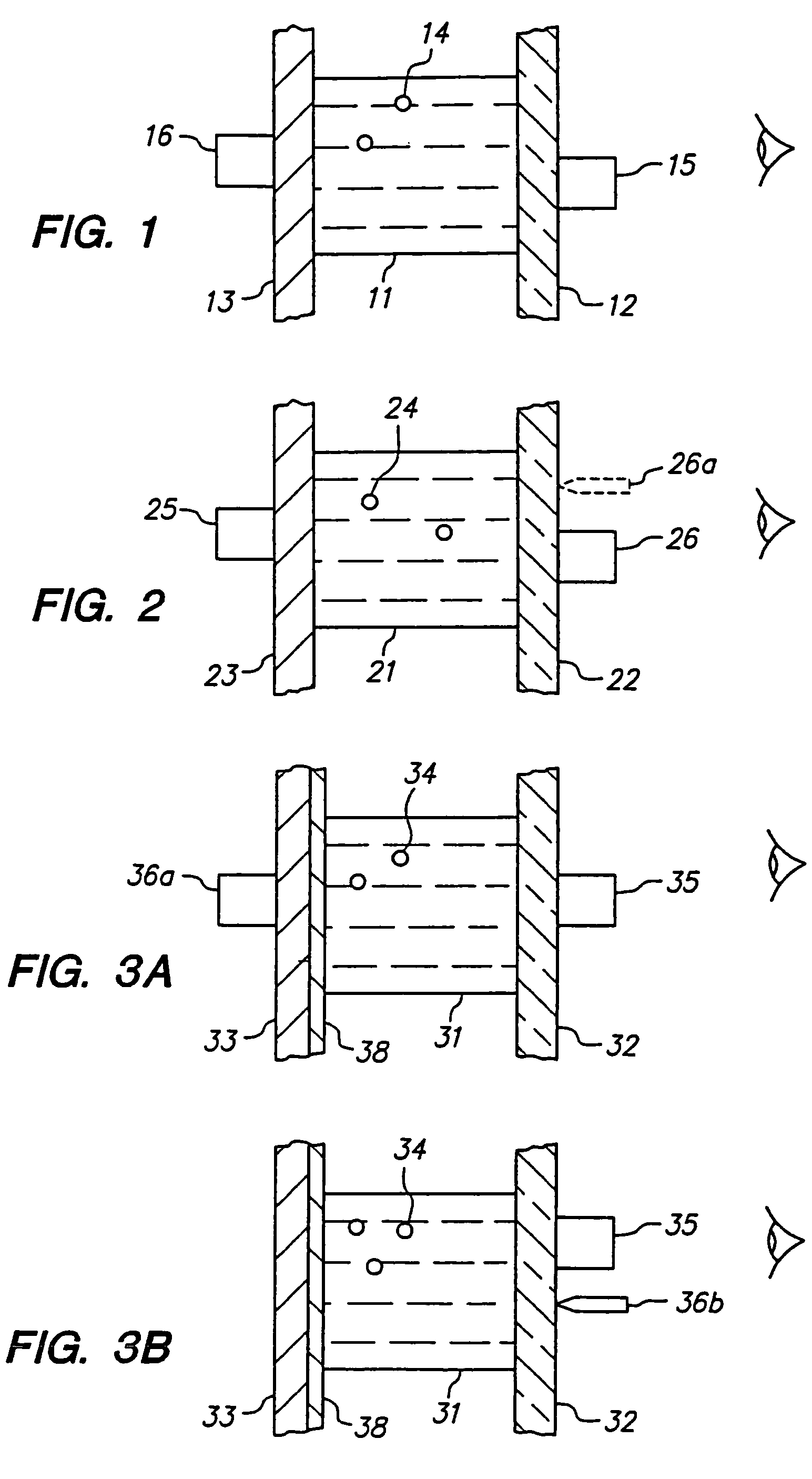
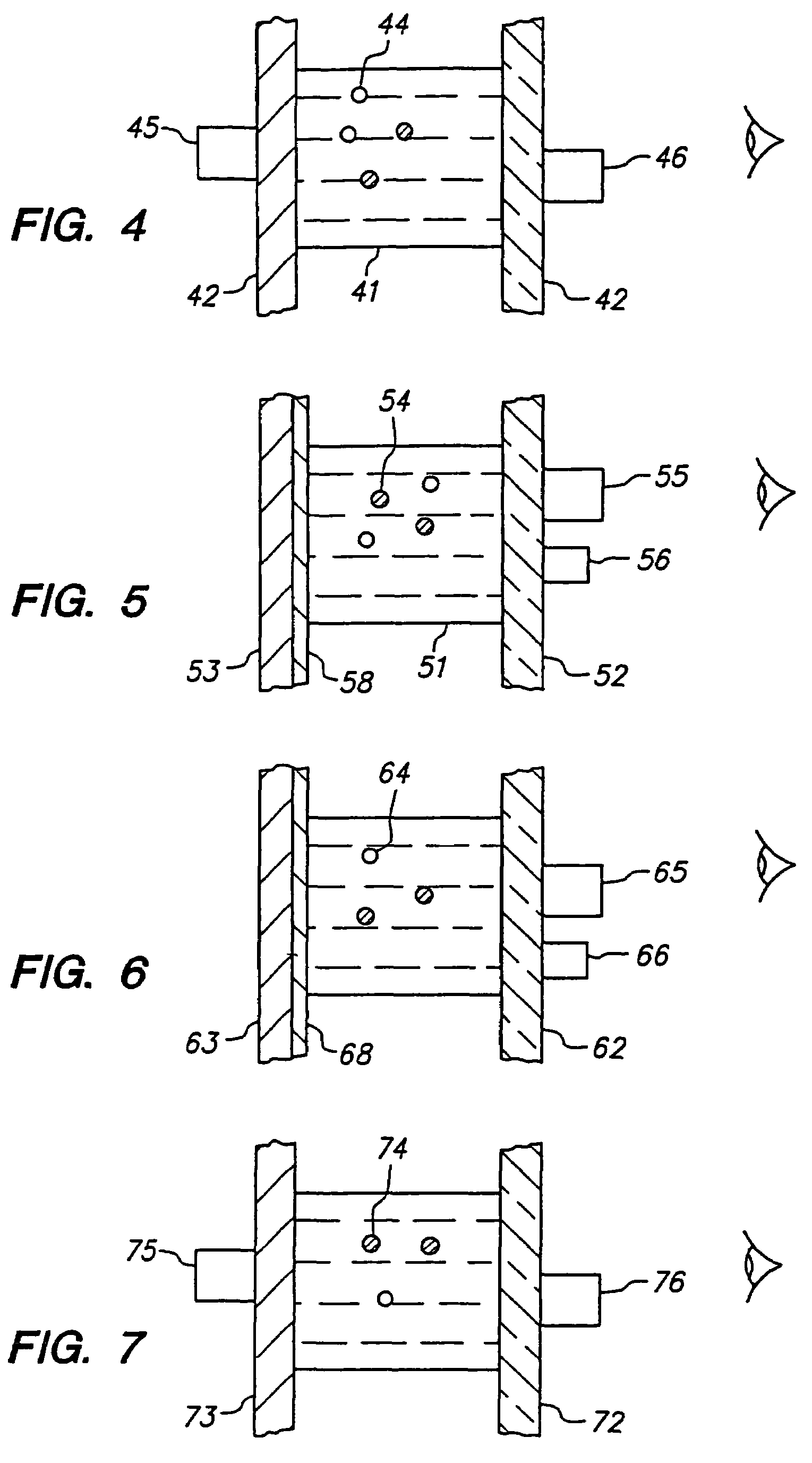
[0017]The present invention is directed to a display device, which comprises two layers of substrate, at least the viewing side is transparent, and an array of display cells sandwiched between the two layers of substrate. In the context of this application, the term “viewing side” refers to the side seen by the viewer whereas the term “non-viewing” side refers to the side opposite from the viewing side.

[0018]In one embodiment, the two substrate layers may be insulating or dielectric layers, such as microporous organosilicates, ceramic, aluminum oxide, titanium dioxide, glass and polymeric sheets, plates or films prepared from poly(ethylene terephthalate), poly(ethylene naphthalate), polycarbonate, polysulfone, polyimide, epoxy, phenolic, acrylics, unsaturated polyester, polyamide, polyurethane, polyurea and composites thereof. In the embodiments of this invention where an electric field is used to drive or erase an image, a conductive layer on the substrate is needed. Suitable condu...


PUM


Abstract

The present invention is directed to a display device which comprises two layers of insulating substrate, at least the substrate on the viewing side is transparent, an array of display cells sandwiched between the two layers of substrate, a writing means, and optionally an erasing means to magnetically or electrically erase the image. The display cells are filled with a dispersion of magnetic particles which may be charged or non-charged. The display of the invention eliminates the use of the transparent conductor film, such as ITO, on the viewing side. Therefore, the displays of this invention are more cost effective, more flexible and durable and capable of higher image contrast ratio and higher reflectance in the Dmin area.

Description

CROSS-REFERENCE TO RELATED APPLICATION[0001]This application is a continuation-in-part of U.S. application Ser. No. 11 / 149,678 filed on Jun. 8, 2005 now U.S. Pat. No. 7,113,323 which is a continuation-in-part of U.S. application Ser. No. 10 / 394,488, filed Mar. 20, 2003, now U.S. Pat. No. 6,927,892, which claims the benefit of U.S. Provisional Application 60 / 367,325, filed Mar. 21, 2002; the contents of all three applications are incorporated herein by reference in their entirety.BACKGROUND OF THE INVENTION[0002]An electrophoretic display (EPD) is a non-emissive device based on the electrophoresis phenomenon influencing charged pigment particles suspended in a colored dielectric solvent. This general type of display was first proposed in 1969. An EPD typically comprises a pair of opposed, spaced-apart plate-like electrodes, with spacers predetermining a certain distance between the electrodes. At least one of the electrodes, typically on the viewing side, is transparent.[0003]When a ...

Claims


Application Information

Patent Timeline
Patent Type & Authority Patents(United States)
IPC IPC(8): G02B26/00G09G3/34
CPCB43L1/008G02F1/09G09F9/375G09F9/372G02F2201/12G02F2001/094G02F1/094
Inventor HO, CHING-SHONCHUNG, JERRYGENDLER, PAULLIANG, RONG-CHANGZANG, HONGMEI
Owner E INK CALIFORNIA
Why Eureka
Try Eureka