Address buffer circuit and method for controlling the same
a buffer circuit and address technology, applied in the direction of information storage, static storage, digital storage, etc., can solve the problems of increasing power consumption, power consumption, and limitation of chip select signal use, and achieve the effect of reducing power consumption
- Summary
- Abstract
- Description
- Claims
- Application Information
AI Technical Summary
Benefits of technology
Problems solved by technology
Method used
Image
Examples
Embodiment Construction
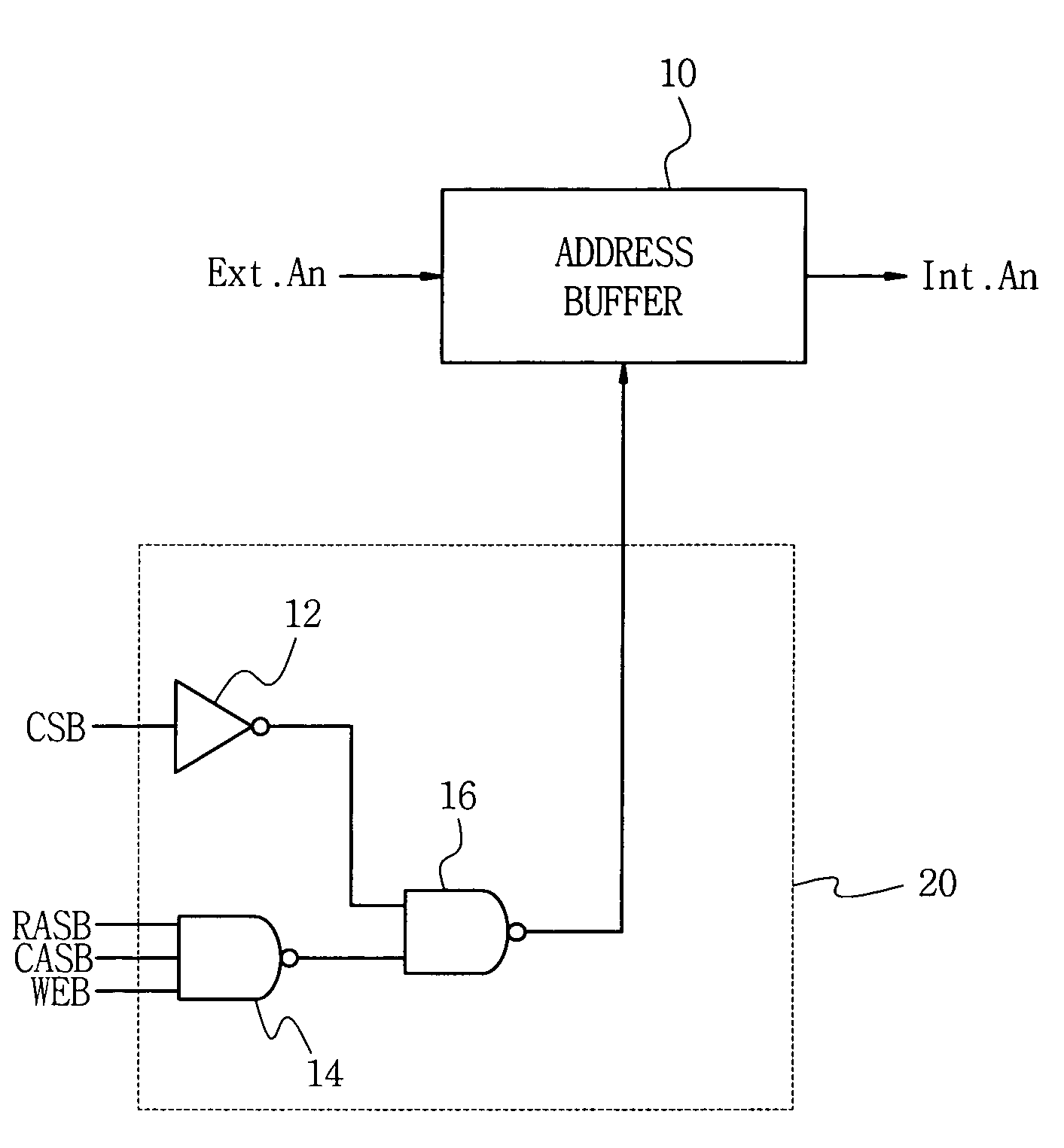
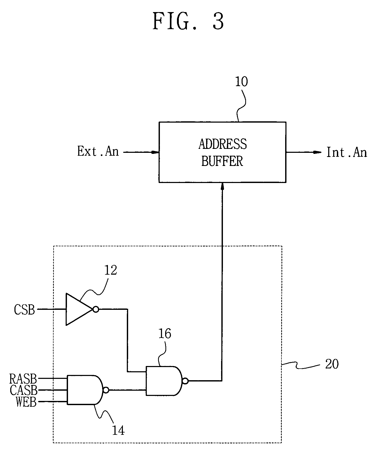
[0050]FIG. 3 is a schematic diagram of an address buffer circuit comprising an address buffer control unit according to an embodiment of the present invention.
[0051]Referring to FIG. 3, there are shown an address buffer 10 that receives and buffers an external address signal and outputs an internal address signal, an external address signal (ext.an) input to the address buffer 10, an internal address signal (Int.an) buffered by and output from the address buffer 10, and an address buffer control unit 20 for controlling the address buffer 10. The address buffer control unit 20 shown in FIG. 3 consists essentially of a combinatorial logic circuit that combines memory control signals (e.g., RASB, CASB, WEB) and a chip select signal (CS). The address buffer control unit 20 includes an inverter 12, a first NAND-gate 14, and a second NAND-gate 16.
[0052]Memory control signals, including a chip select signal (CSB), a row address strobe (RASB), a column address strobe (CASB), a write enable ...
PUM
 Abstract
Description
Claims
Application Information


