Structure and assembly procedure for low stress thin die flip chip packages designed for low-K Si and thin core substrate

a technology of thin-die flip chip and assembly procedure, which is applied in the direction of semiconductor devices, semiconductor/solid-state device details, electrical apparatus, etc., can solve the problems of brittle low-k dielectric materials in low-k si dice, adversely affecting the board level reliability of the package, and affecting the stability of the package, so as to facilitate the management of package stress and minimize the stress generated/experienced by the die

Inactive Publication Date: 2009-09-08
ALTERA CORP
View PDF29 Cites 33 Cited by
  • Summary
  • Abstract
  • Description
  • Claims
  • Application Information

AI Technical Summary

Benefits of technology

[0006]To achieve the foregoing, the present invention provides a semiconductor die flip chip package and a semiconductor die flip chip package component where aspects of the package and the component are controlled to facilitate management of the package stress. The present invention also provides fabrication methods for such packages. For instance, the thickness of the die can be controlled such that the stress generated / experienced by the die is minimized. As such, the package stress is managed to suitable levels for incorporation of a low-K Si die and / or a thin package substrate.

Problems solved by technology

A problem with such a semiconductor die flip chip package is that it is subject to different temperatures during the packaging process.
The high stress experienced by bonded materials during cooling may cause them to warp or crack and cause the package structure to bow, thereby, adversely affecting the board level reliability of the package.
However, as compared to traditional dielectric materials in conventional silicon based dice, the low-K dielectric materials in low-K Si dice are brittle and tend to crack under substantially less stress.
As such, it is possible for the reliability of a low-K Si die to be compromised due to cracking of the low-K dielectric material.
As such, the CTE mismatches between the die, bumps, underfill, package substrate, and BGA balls can cause earlier failures in a semiconductor die flip chip package during board level reliability tests.

Method used


Image

  • Structure and assembly procedure for low stress thin die flip chip packages designed for low-K Si and thin core substrate
  • Structure and assembly procedure for low stress thin die flip chip packages designed for low-K Si and thin core substrate
  • Structure and assembly procedure for low stress thin die flip chip packages designed for low-K Si and thin core substrate

Examples


Embodiment Construction

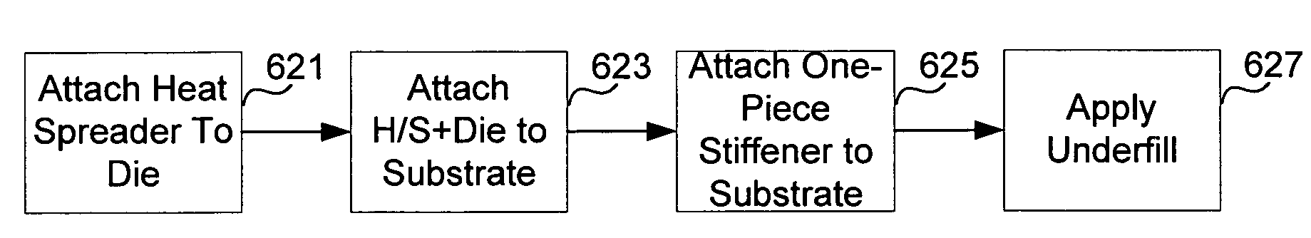
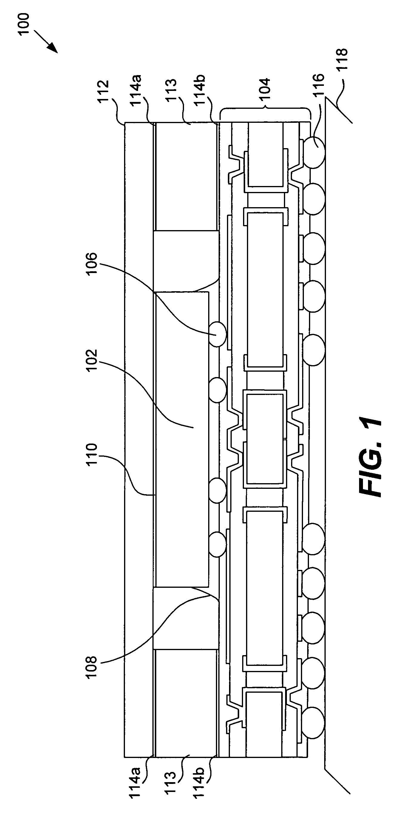
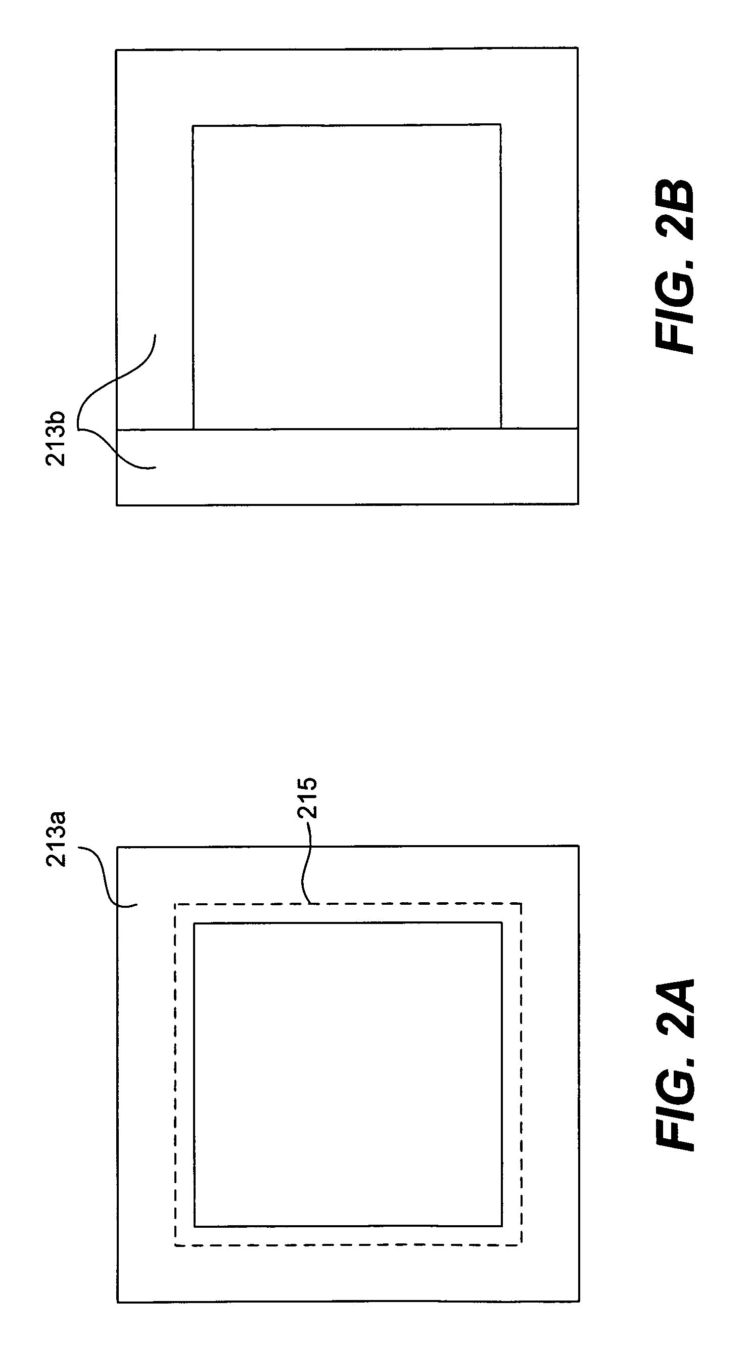
[0033]Reference will now be made in detail to specific embodiments of the invention. Examples of the specific embodiments are illustrated in the accompanying drawings. While the invention will be described in conjunction with these specific embodiments, it will be understood that it is not intended to limit the invention to such specific embodiments. On the contrary, it is intended to cover alternatives, modifications, and equivalents as may be included within the spirit and scope of the invention as defined by the appended claims. In the following description, numerous specific details are set forth in order to provide a thorough understanding of the present invention. The present invention may be practiced without some or all of these specific details. In other instances, well known process operations have not been described in detail in order not to unnecessarily obscure the present invention.

[0034]Provided are semiconductor die flip chip packages and semiconductor die flip chip ...


PUM


Abstract

Provided are semiconductor die flip chip packages and semiconductor die flip chip package components where certain properties of the packages/components are controlled to facilitate management of the package stresses. Also provided are fabrication methods for such packages and package components. For instance, the thickness of a die can be controlled such that the stress generated/experienced by the die is minimized. As such, the package stress is managed to suitable levels for incorporation of a low-K Si die and/or a thin package substrate. Further, a thin die can be attached to a heat spreader to increase the rigidity for easier handling during fabrication of the semiconductor die flip chip package.

Description

BACKGROUND[0001]This invention relates generally to semiconductor device packages, and in particular to semiconductor die flip chip packages. More specifically, the invention relates to structures and assembly procedures for low stress thin die flip chip packages suited for low-K Si dice and / or thin core substrates.[0002]In semiconductor device package assembly, a semiconductor die (also referred to as an integrated circuit (IC) chip or “chip”) may be bonded directly to a package substrate. Such die is formed with bumps of solder affixed to its I / O bonding pads. During conventional packaging assembly, the die is “flipped” onto its front surface (e.g., active circuit surface) so that the solder bumps form electrical and mechanical connections directly between the die and conductive metal pads on the package substrate. Underfill is then applied between the gap formed by the solder bumps in order to further secure the die to the package substrate. Next, a stiffener made of substantiall...

Claims


Application Information

Patent Timeline
Patent Type & Authority Patents(United States)
IPC IPC(8): H01L21/44
CPCH01L21/50H01L23/16H01L23/3128H01L21/563H01L2224/73204H01L2224/32225H01L2224/16225H01L2924/01322H01L2924/01019H01L2924/16195H01L2924/15311H01L2924/14H01L2924/10253H01L2924/0102H01L24/31H01L24/81H01L2224/73253H01L2224/81801H01L2924/00H01L2924/3512
Inventor WANG, WEN-CHOU VINCENTLI, YUANEUZENT, BRUCEMAHADEV, VADALI
Owner ALTERA CORP
Why Eureka
Try Eureka