Semiconductor memory device

a memory device and semiconductor technology, applied in the direction of information storage, static storage, digital storage, etc., can solve the problems of increasing the margin (static noise margin) for erroneous writing due to bit-line noise or the like, and become extremely difficult to design a memory cell having stable characteristics, etc., to achieve the effect of enlargement of the operation margin of the memory cell

Inactive Publication Date: 2009-09-08
SOCIONEXT INC
View PDF7 Cites 7 Cited by
  • Summary
  • Abstract
  • Description
  • Claims
  • Application Information

AI Technical Summary

Benefits of technology

[0036]The present invention has been achieved by focusing attention on the problems described above and it is therefore an object of the present invention to provide a semiconductor memory device comprising flip-flop memory cells such as SRAMs which allows enlargement of the operation margins of the memory cells.

Problems solved by technology

Under the adverse effects thereof, in a semiconductor memory device comprising flip-flop memory cells such as, e.g., a static random access memory (SRAM), it has become extremely difficult to design a memory cell having stable characteristics due to variations in the characteristics of individual transistors composing the memory cell and the lower power source voltage.
As a result, a lower production yield of the semiconductor memory device resulting from the degraded operation margins of the memory cell has presented a problem.
For example, when the write margin is low, the margin (static noise margin) for erroneous writing due to bit-line noise or the like increases.
On the other hand, when the potential of the bit line has not reached a sufficiently low level, the flip-flop cannot be inverted.
Conversely, when the write margin is high, the time required for data writing is reduced, but the margin for erroneous writing (static noise margin) decreases.
On the other hand, a high write margin indicates that the state of the flip-flop composing the memory cell is susceptible to inversion during a read operation, i.e., the static noise margin decreases.
When the potential on the word line WL is increased or the threshold of each of the drive transistors or the access transistors is lowered with the view to increasing the reading speed, data at the storage nodes of the flip-flop is more susceptible to the influence of the bit-line noise so that the static noise margin lowers.
However, when the cell current is increased by reducing the threshold of each of the memory cell transistors or increasing the word line potential, the susceptibility to the bit-line noise increases and the static noise margin decreases.
In other words, the static noise margin is thereby increased.
However, there is the problem that data writing during a write operation becomes difficult, while the cell current during a read operation decreases to reduce the reading speed.
It is also expected that, as variations in the thresholds of transistors further increase with future process miniaturization, the static noise margin of the SRAM memory cell further decreases.
However, when the word line potential is further lowered, the problem is encountered that the Low level cannot be written in the memory cell even if the bit line potential is lowered to 0 V during a write operation, while the reading speed is further reduced.
As a result, the problem occurs that the power source voltage for holding data in the non-selected memory cells decreases to result in data destruction.
There is also the problem that, although the static noise margin is increased by increasing the threshold voltage of each of the memory cell transistors to a level higher than that of the threshold voltage of each of the logic transistors, the write margin and the cell current are conversely reduced by the increased threshold voltage.
In addition, to increase the threshold voltage, the process step of adjusting an impurity only for the threshold adjustment of the memory cells is necessary, which leads to the problem of higher process cost.
There is the further problem that, when the impurity in each of the memory cell transistors is increased to increase the threshold voltage thereof, variations in the threshold voltages of the transistors increase to reduce the operation margins of the memory cells.
Thus, in the conventional semiconductor memory device, when one of the operation margins of the SRAM memory cell is to be improved, the other operation margins deteriorate under the constraints of the tradeoff relations among the operation margins.
This results in the problem that, to satisfy all of the operation margins, optimization design should be performed under operating conditions in an extremely narrow range.
There is also the problem that, to obtain a margin during data writing, the contradictory characteristics of: (2) write margin; and (4) data holding voltage should be optimized.
There is the further problem that, as variations in the threshold voltages of transistors increase with future process miniaturization, a design range capable of satisfying these characteristics is further narrowed, and the design of the SRAM memory cell becomes difficult.

Method used


Image

  • Semiconductor memory device
  • Semiconductor memory device
  • Semiconductor memory device

Examples


embodiment 1

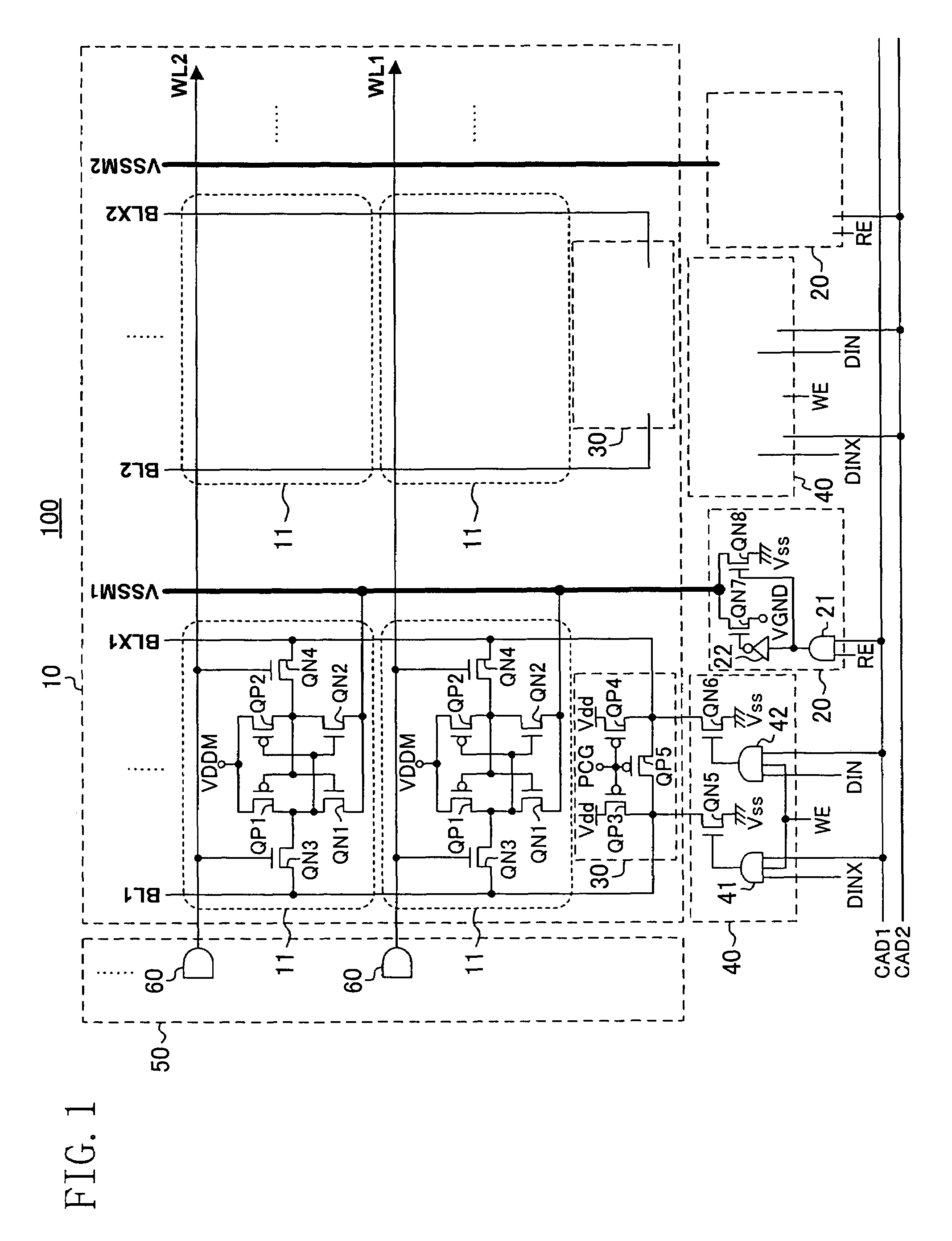
[0055]A semiconductor memory device 100 according to a first embodiment of the present invention will be described with reference to FIGS. 1 to 4.

(Structure of Semiconductor Memory Device 100)

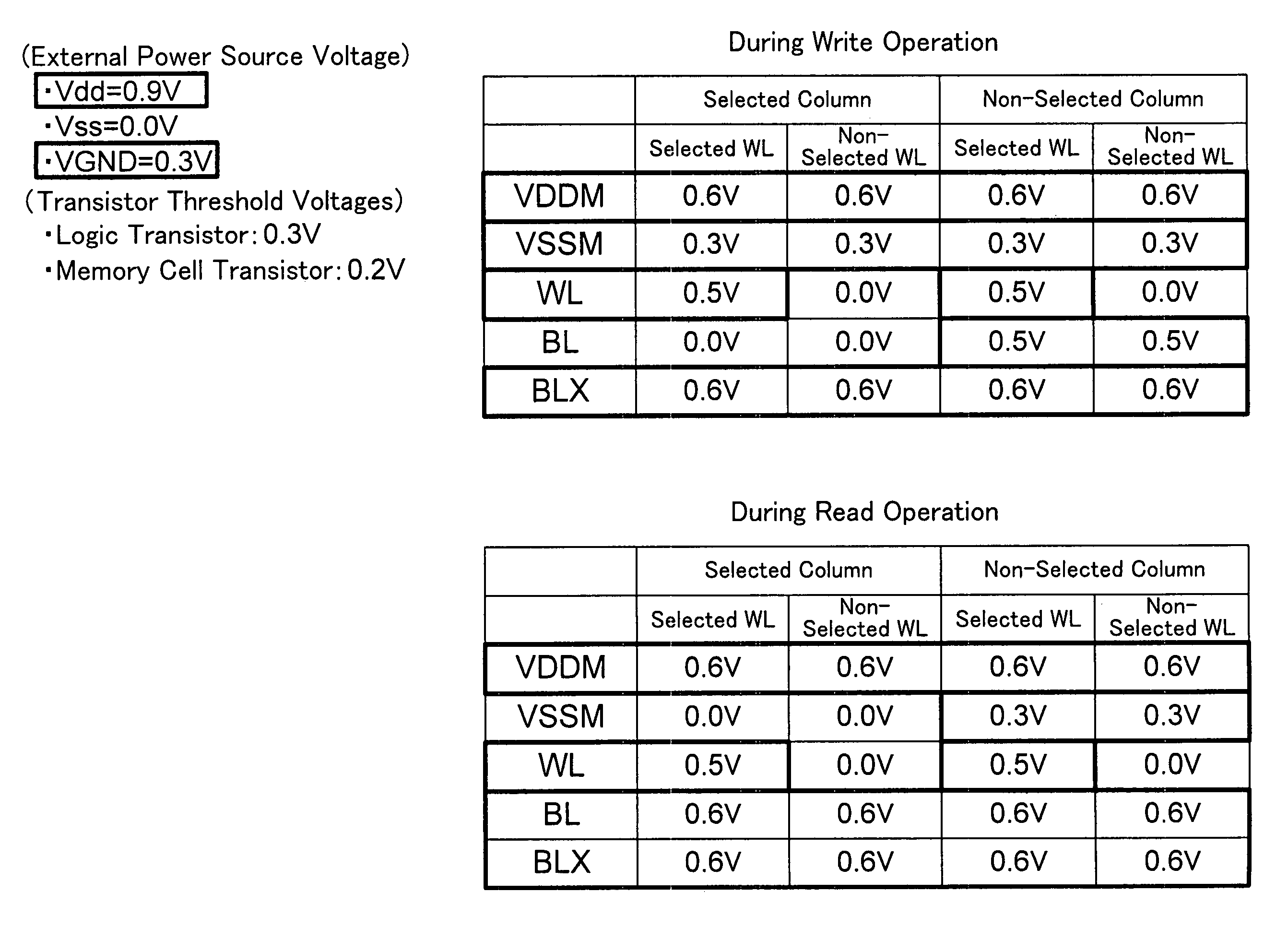
[0056]FIG. 1 is a block diagram showing a structure of a semiconductor memory device 100. For easier illustration, an output-system circuit such as a sense amplifier is omitted in FIG. 1.

[0057]As shown in FIG. 1, the semiconductor memory device 100 comprises a plurality of Low-data-holding power source control circuits 20, a plurality of bit-line precharge circuits 30, a plurality of write control circuits 40, a memory cell array 10, and a row decoder 50.

[0058]In FIG. 1, WL1 and WL2 denote word lines each routed to extend in a row direction.

[0059]BL1, BL2, BLX1, and BLX2 denote bit lines each routed to extend in a column direction. The bit lines BL1 and BLX form a bit line pair, while the bit lines BL2 and BLX2 form a bit line pair.

[0060]PCG denotes a signal (precharge control signal PCG) trans...

embodiment 2

[0127]Next, a semiconductor memory device 200 according to a second embodiment of the present invention will be described with reference to FIGS. 5 and 6.

[0128]FIG. 5 is a block diagram showing a structure of the semiconductor memory device 200. For easier illustration, an output-system circuit such as a sense amplifier is also omitted in FIG. 5.

[0129]Specifically, the semiconductor memory device 200 has been obtained by replacing the bit-line precharge circuits 30 of the semiconductor memory device 100 with bit-line precharge circuits 210, adding a PMOS transistor QP20, and further changing the threshold voltage of each of the transistors of the memory cells 11.

[0130]The bit line precharge circuits 210 have been obtained by setting the source power source of each of the precharge transistors QP3 and QP4 in the bit-line precharge circuits 30 to the potential VGND (0.5 V). That is, the structure of each of the transistors of the bit-line precharge circuits 210 is the same as the stru...

embodiment 3

[0146]Next, a semiconductor memory device 300 according to a third embodiment of the present invention will be described with reference to FIGS. 7 to 11.

(Structure of Semiconductor Memory Device 300)

[0147]FIG. 7 is a block diagram showing a structure of the semiconductor memory device 300 according to the third embodiment. For easier illustration, an output-system circuit such as a sense amplifier is also omitted in FIG. 7.

[0148]The semiconductor memory device 300 has been constructed by replacing the bit-line precharge circuits 210 of the semiconductor memory device 200 with bit-line precharge circuits 310, replacing the row decoder 50 with a row decoder 320, replacing the Low-data-holding-power-source control circuits 20 with Low-data-holding-power-source control circuits 340, and adding an NMOS transistor QN30.

[0149]The NMOS transistor QN30 is a transistor disposed on the periphery of the memory cell array 10 to generate the potential VGND. The source of the NMOS transistor QN30 ...


PUM


Abstract

In a semiconductor memory device including memory cells each having two inverters connected in a cross-coupled configuration to hold High data and Low data as a pair and two access transistors, a plurality of word lines, and a plurality of bit lines, the potential of the selected one of the plurality of word lines is controlled to be lower than a potential obtained by adding up the potential of one of Low-data-holding power sources each for holding the Low data at any time other than during a read operation and the threshold voltage of each of the access transistors.

Description

BACKGROUND OF THE INVENTION[0001]1. Field of the Invention[0002]The present invention relates to a semiconductor memory device comprising flip-flop memory cells.[0003]2. Description of the Prior Art[0004]With the recent process miniaturization, there have been rapidly growing tendencies toward a smaller-area semiconductor integrated circuit and a lower power source voltage. Under the adverse effects thereof, in a semiconductor memory device comprising flip-flop memory cells such as, e.g., a static random access memory (SRAM), it has become extremely difficult to design a memory cell having stable characteristics due to variations in the characteristics of individual transistors composing the memory cell and the lower power source voltage. As a result, a lower production yield of the semiconductor memory device resulting from the degraded operation margins of the memory cell has presented a problem.[0005]The operation margins of the memory cell mentioned herein include a write margin...

Claims


Application Information

Patent Timeline
Patent Type & Authority Patents(United States)
IPC IPC(8): G11C7/00
CPCG11C11/413G11C11/412
Inventor SUZUKI, TOSHIKAZU
Owner SOCIONEXT INC
Why Eureka
Try Eureka