Method for fabricating lateral semiconductor device
a semiconductor device and lateral junction technology, applied in semiconductor devices, semiconductor lasers, lasers, etc., can solve the problems of increasing the radiative recombination time, limiting the modulation bandwidth, and limiting the conventional, or vertical, p-n junctions of light-emitting devices such as transistors or resistors
- Summary
- Abstract
- Description
- Claims
- Application Information
AI Technical Summary
Benefits of technology
Problems solved by technology
Method used
Image

Examples
first embodiment
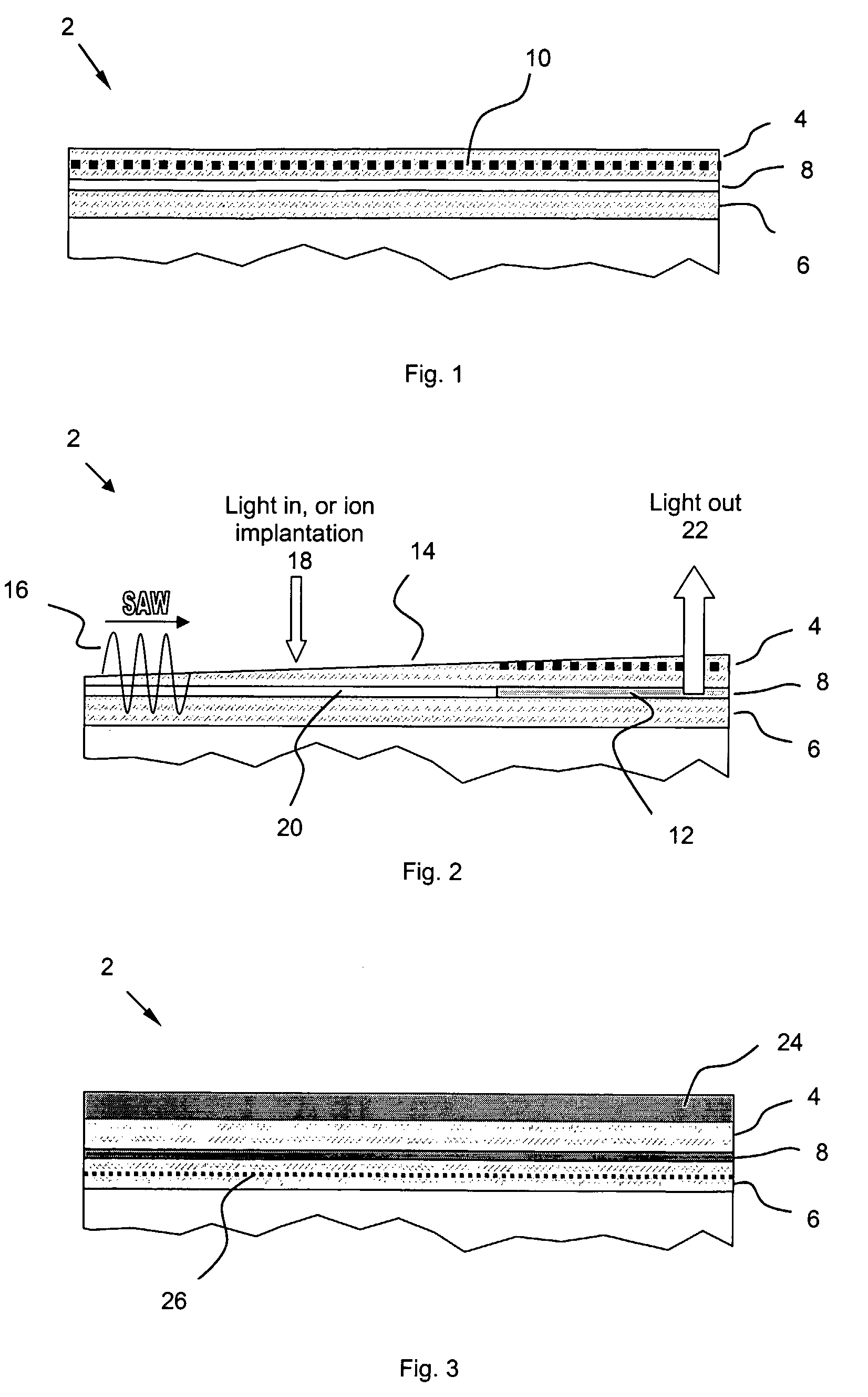
[0076]Referring to FIGS. 1 and 2, the invention shall now be described comprising a single photon source device and method for fabricating the same. The device 2 is based on epitaxial growth of semiconductor layers onto a single crystal substrate, and a schematic cross-section of the proposed device after growth is shown in FIG. 1. The top 4 and bottom 6 layers are grown such that they have a larger bandgap than the middle layer 8. This is achieved by growing layers of different composition so, for example, the top and bottom layers shall be AlGaAs, and the middle layer GaAs. Other suitable material systems include, but are not limited to, Hg1-xCdxTe and InGaAs / InGaAsP.
[0077]The device 2 illustrated in FIG. 1 utilises a quantum well structure wherein the carrier wavefunction falls rapidly to zero away from the middle layer. The electrons (or holes) in the quantum well form a 2D sheet by mainly occupying the lowest energy standing wave in the direction perpendicular to the plane of t...
second embodiment
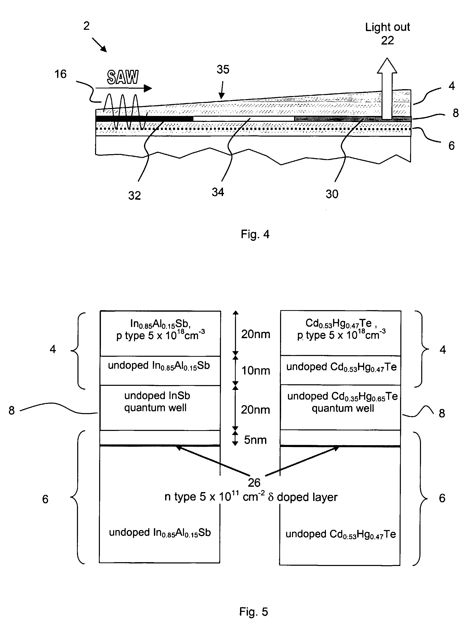
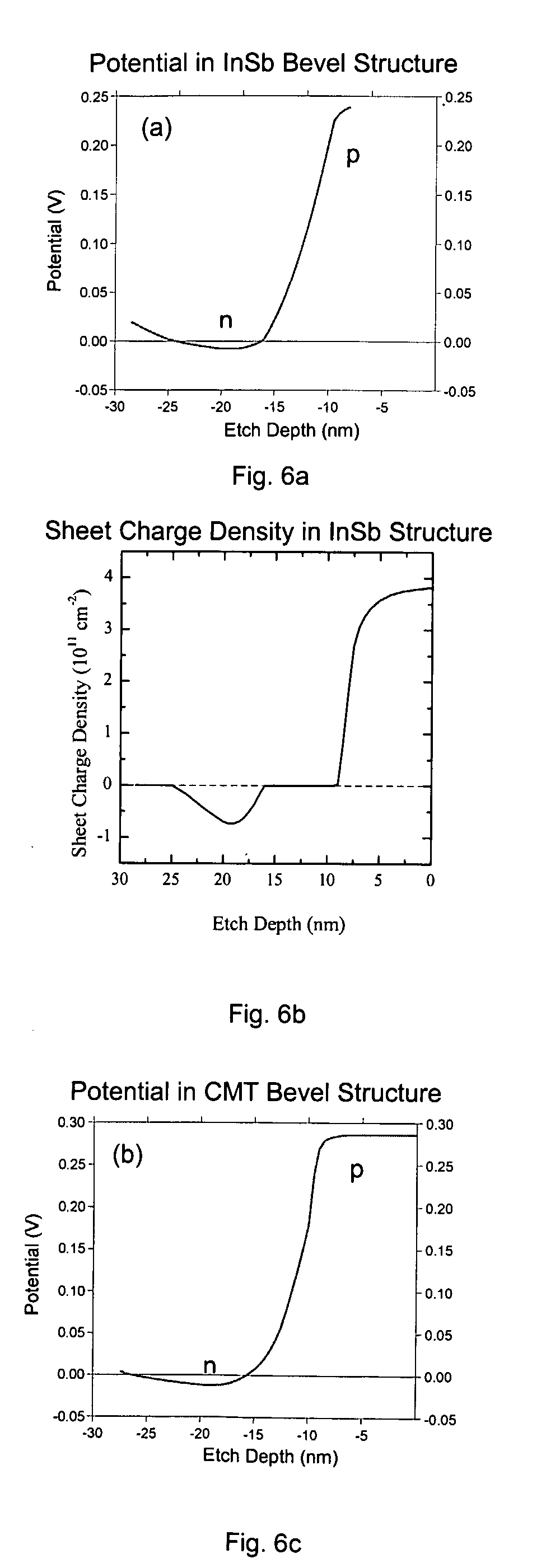
[0082]Referring now to FIGS. 3 and 4, the invention shall now be described comprising an alternative single photon source 2 device to that described in the foregoing and method for fabricating the same. To avoid unnecessary repetition, like features which have been described with reference to FIGS. 1 and 2 have been give the same reference numerals.
[0083]The development of true photon sources is of fundamental scientific and technological importance, and in this second embodiment of the present invention single electrons are injected into the p-type region of a lateral p-i-n junction. In this embodiment the single photon source 2 is electrically driven. The device has potential advantages over conventional sources, namely the potential to operate at relatively high frequencies, the ability to produce many parallel photon trains, and the possibility that single photons are emitted with a known polarisation (the latter two are highly desirable properties with respect to quantum crypto...
PUM
 Abstract
Description
Claims
Application Information
 - R&D
- Intellectual Property
- Life Sciences
- Materials
- Tech Scout
- Unparalleled Data Quality
- Higher Quality Content
- 60% Fewer Hallucinations
Browse by: Latest US Patents, China's latest patents, Technical Efficacy Thesaurus, Application Domain, Technology Topic, Popular Technical Reports.
© 2025 PatSnap. All rights reserved.Legal|Privacy policy|Modern Slavery Act Transparency Statement|Sitemap|About US| Contact US: help@patsnap.com