Photoelectric conversion device having plural pixel columns and independent readout wiring, multichip image sensor, contact image sensor, and image scanner

a conversion device and photoelectric technology, applied in the field of photoelectric conversion devices, can solve the problems of reducing sensitivity, affecting image quality, and generating differences in sensitivity in each pixel column, so as to suppress the decrease in sensitivity, the difference in capacitance, and the effect of reducing sensitivity

Inactive Publication Date: 2009-09-22
CANON KK
View PDF25 Cites 7 Cited by
  • Summary
  • Abstract
  • Description
  • Claims
  • Application Information

AI Technical Summary

Benefits of technology

[0023]In view of the foregoing, an object of the invention is to provide a photoelectric conversion device which suppresses the difference in sensitivity among the pixel columns and the decrease in sensitivity, caused by the capacitance associated with the photoelectric conversion device.
[0024]Another object of the invention is to provide a photoelectric conversion device in which the crosstalk between the wirings to eliminate the color mixture or to obtain the high-quality image without generating the decrease in contrast.
[0030]According to the invention, the difference in sensitivity caused by the difference in capacitance between the columns associated with the photodiode and the decrease in sensitivity can be suppressed.
[0031]According to the invention, the signal crosstalk can be prevented between the readout wirings to eliminate the color mixture or to obtain the high-quality image without generating the decrease in contrast.
[0032]According to the invention, a signal fluctuation to the storage capacitance caused by the fluctuation in wiring length can be suppressed by keeping the wiring length constant between the source follower current source and the signal transfer transistor.

Problems solved by technology

However, the following problems are generated when the pixels are arranged as shown in FIG. 9.
When the pixel columns differ from one another in the wiring capacitance of the readout wiring 16, there is the problem that a difference in sensitivity is generated in each pixel column.
The total capacitance associated with the photodiode PD is increased by providing the readout wiring 16 to the readout circuit block 3, which results in the problem that the sensitivity is decreased.
Therefore, a crosstalk is generated by a parasitic capacitance between the readout wirings 16 (for example, between the readout wiring 16g1 and 16b2), which leads to color mixture to generate the problem that image quality is remarkably decreased in the color image.
This is the new problem which is not generated in the case of an area sensor.
However, in the case of the multichip module type image sensor, the vertical shift register cannot be arranged because the pixel column is arranged to an edge portion of the chip.
Therefore, it is difficult to avoid the above problem.
The crosstalk problem is not limited to the sensor on which the color filter is mounted.
Accordingly, when the wirings are arranged adjacent to each other, there is generated the problem that the generation of the crosstalk worsens image contrast.

Method used


Image

  • Photoelectric conversion device having plural pixel columns and independent readout wiring, multichip image sensor, contact image sensor, and image scanner
  • Photoelectric conversion device having plural pixel columns and independent readout wiring, multichip image sensor, contact image sensor, and image scanner
  • Photoelectric conversion device having plural pixel columns and independent readout wiring, multichip image sensor, contact image sensor, and image scanner

Examples


first embodiment

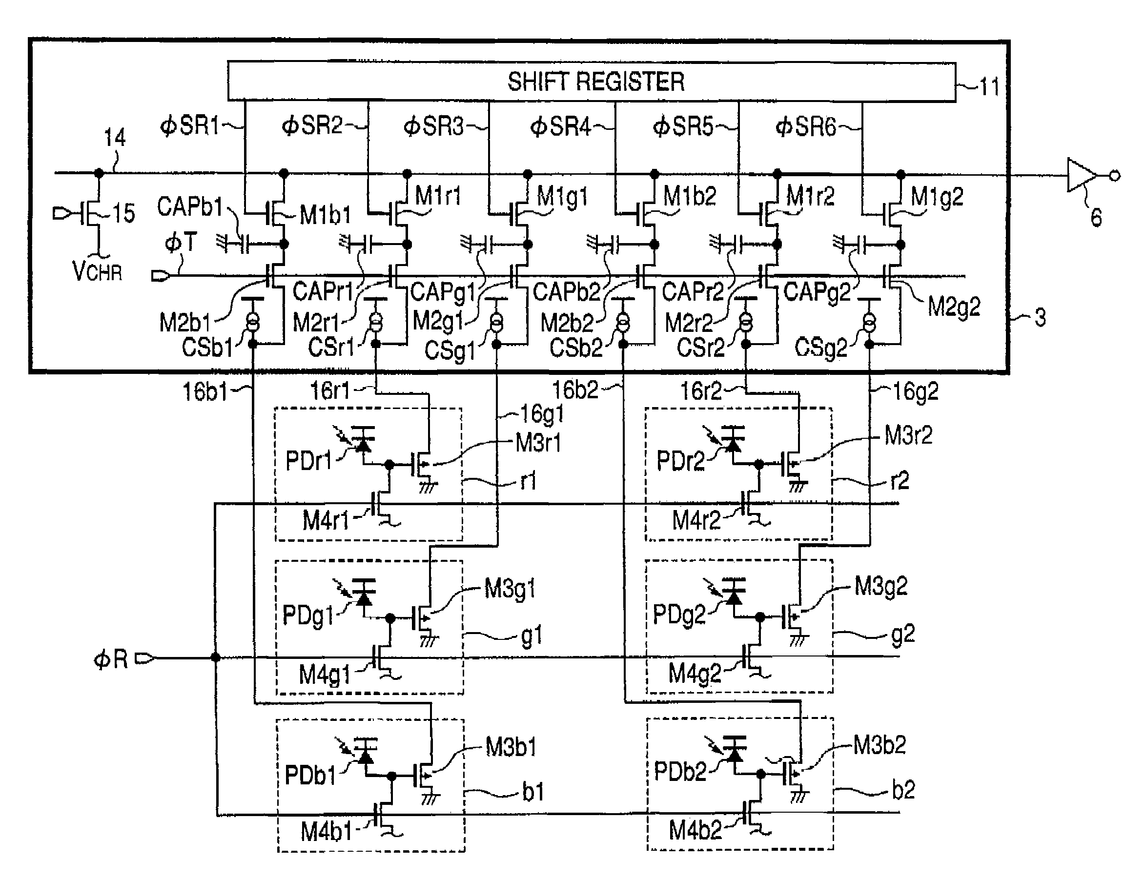
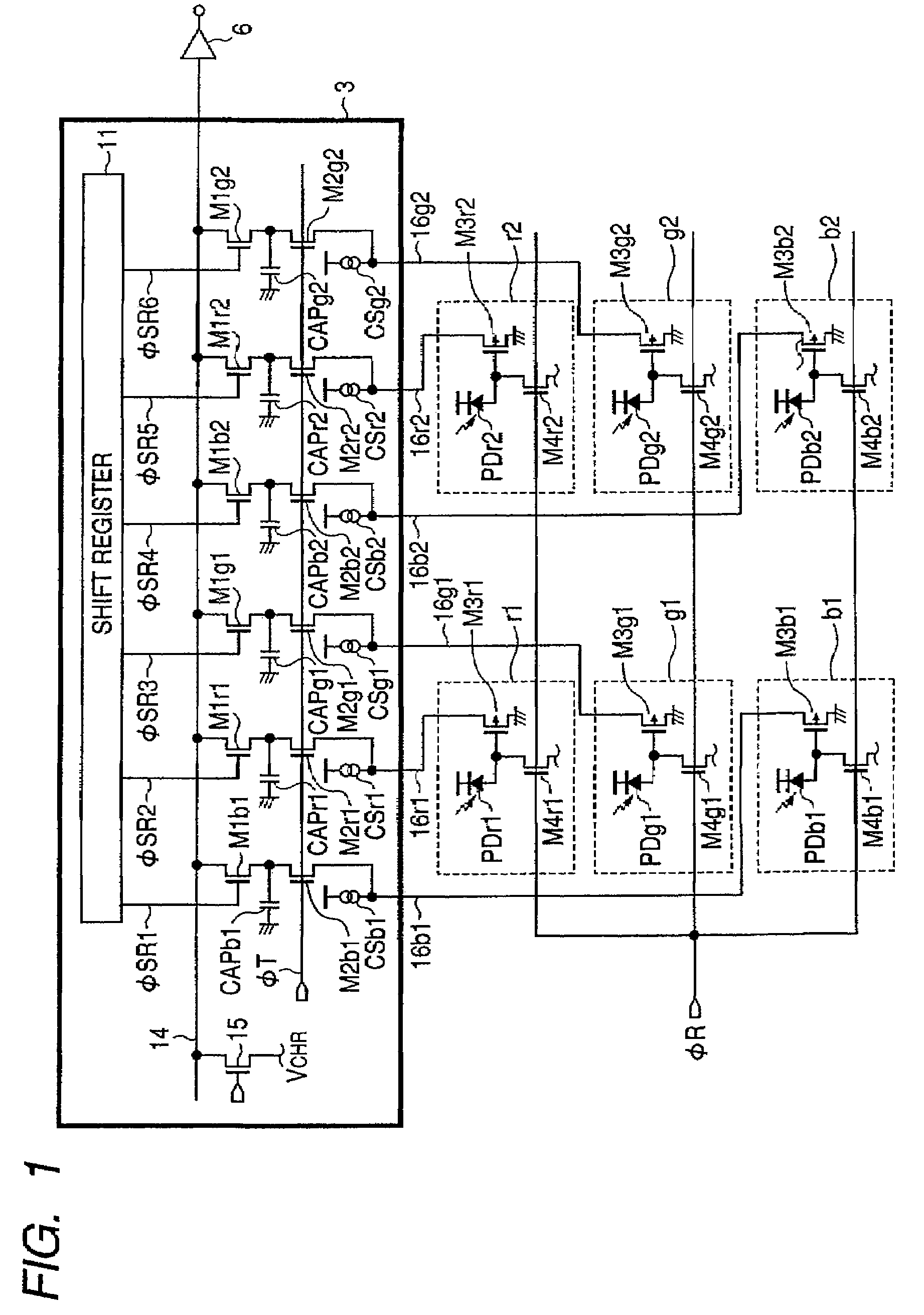
[0047]FIG. 1 shows a configuration of a light receiving element according to a first embodiment of the invention. FIG. 1 shows an equivalent circuit corresponding to the readout circuit block 3 and light receiving element array 4 (only two-pixel-by-three-column light receiving element (three pixel columns) is shown) shown in FIG. 6. The equivalent circuit of the color image sensor in the first embodiment is similar to the equivalent circuit diagram shown in FIG. 6, and the configuration and the operation are already described, so that the description will be not repeated. In FIG. 1, the component similar to that of FIG. 8 is designated by the same reference numeral or sign.

[0048]Referring to FIG. 1, the light receiving elements (constituting the pixel) r1 to b2 include the photodiode PDr1 to PDb2 which are of the photoelectric conversion element, the MOS source follower input transistors M3r1 to M3b2, and the reset switches (reset transistors) M4r1 to M4b2 which are of the means for...

second embodiment

[0058]FIG. 3 shows a configuration of a light receiving element according to a second embodiment of the invention. FIG. 3 shows an equivalent circuit corresponding to the readout circuit block 3 and light receiving element array 4 (only two-pixel-by-three-column light receiving element is shown) shown in FIG. 6. The equivalent circuit of the color image sensor in the second embodiment is similar to the equivalent circuit diagram shown in FIG. 6, and the configuration and the operation are already described, so that the description will be not repeated. In FIG. 1, the component similar to that of FIG. 8 is designated by the same reference numeral or sign.

[0059]In the second embodiment, the invention is applied to the photoelectric conversion device having a depletion transfer type pixel. In FIG. 3, second signal transfer switches M6r1 to M6b2 are collectively turned on, and the signal charges are collectively and completely depletion-transferred from the photodiodes PDr1 to PDb2 to t...

third embodiment

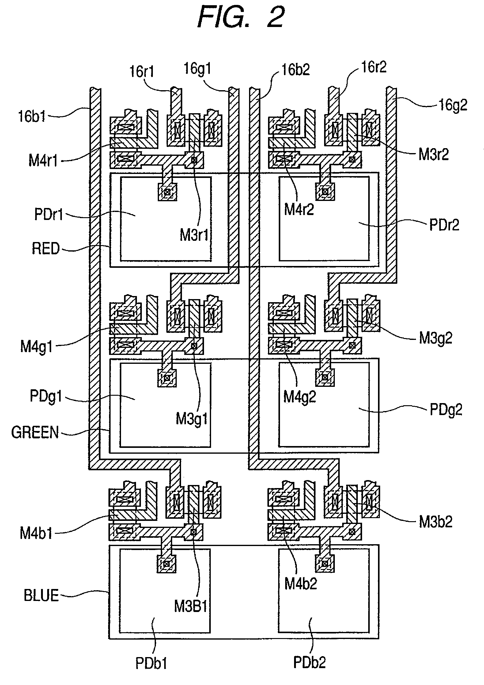
[0069]FIG. 5 shows a photoelectric conversion device according to a third embodiment of the invention. The six-column light receiving element is configured so as to output the light signals while the six-column light receiving element is divided into each three columns of upper and lower portions. The reference numeral 1101 denotes a light receiving element, the reference numerals 3-1 and 3-2 designate a readout circuit block, and the reference numeral 6 denotes a signal output amplifier. The three-column light receiving element column is described in the first and second embodiments. However, as the number of pixel columns is increased as shown in FIG. 5, the number of readout wirings 16 running between the light receiving elements is increased. Therefore, it is necessary to secure the wiring area by decreasing an aperture area of the photodiode, which decreases the sensitivity. However, in the third embodiment, even if the number of light receiving element columns doubles the firs...


PUM


Abstract

The invention provides a photoelectric conversion device, in which a decrease in sensitivity and a crosstalk between wirings are suppressed. Plural pixel columns are arranged in one direction, plural pixels are arranged in a different direction to the one direction in a column manner in the pixel column, and the pixel includes a photodiode PD, a reset transistor M4 for resetting the photodiode PD, and a source follower input transistor M3 for receiving a signal from the photodiode PD. An independent readout wiring 16 is individually provided for each pixel. The reset transistor M4 and the source follower input transistor M3 included in one pixel column or another pixel column are arranged between the photodiode column in one pixel column and the photodiode column in another pixel column arranged adjacent to the one pixel column.

Description

BACKGROUND OF THE INVENTION[0001]1. Field of the Invention[0002]The present invention relates to a photoelectric conversion device in which plural pixel columns, in which plural pixels are arrayed, are arranged and an independent readout wiring is individually provided for each pixel. The invention also relates to a multichip module type image sensor, a contact image sensor, and an image scanner on which the plural photoelectric conversion devices are mounted.[0003]2. Related Background Art[0004]Recently, in an information processing field, in contrast to the conventional scaling-system line sensor in which an optical system is used, the same-magnification system contact image sensor on which plural image sensor chips are multichip-mounted is actively developed as the line image scanner.[0005]For example, Japanese Patent Application Laid-Open No. H11-234472 discloses a structure of the contact image sensor in which the image sensor chips having one-line light receiving element array...

Claims


Application Information

Patent Timeline
Patent Type & Authority Patents(United States)
IPC IPC(8): H01L27/00
CPCH01L27/14601H01L27/14645H04N3/155H04N5/3741H04N5/335H04N5/3591H04N3/1568H04N25/621H04N25/766H04N25/75H04N25/00
Inventor KOCHI, TESTSUNOBU
Owner CANON KK
Why Eureka
Try Eureka