Resonant gate drive circuits

a gate drive and circuit technology, applied in the direction of electronic switching, efficient power electronics conversion, pulse technique, etc., can solve the problems of gate drive loss, gate drive loss increase, and penalty on overall converter efficiency. significant, so as to reduce gate drive loss and other losses.

Inactive Publication Date: 2009-10-06
GANPOWER SEMICON FOSHAN LTD
View PDF14 Cites 17 Cited by
  • Summary
  • Abstract
  • Description
  • Claims
  • Application Information

AI Technical Summary

Benefits of technology

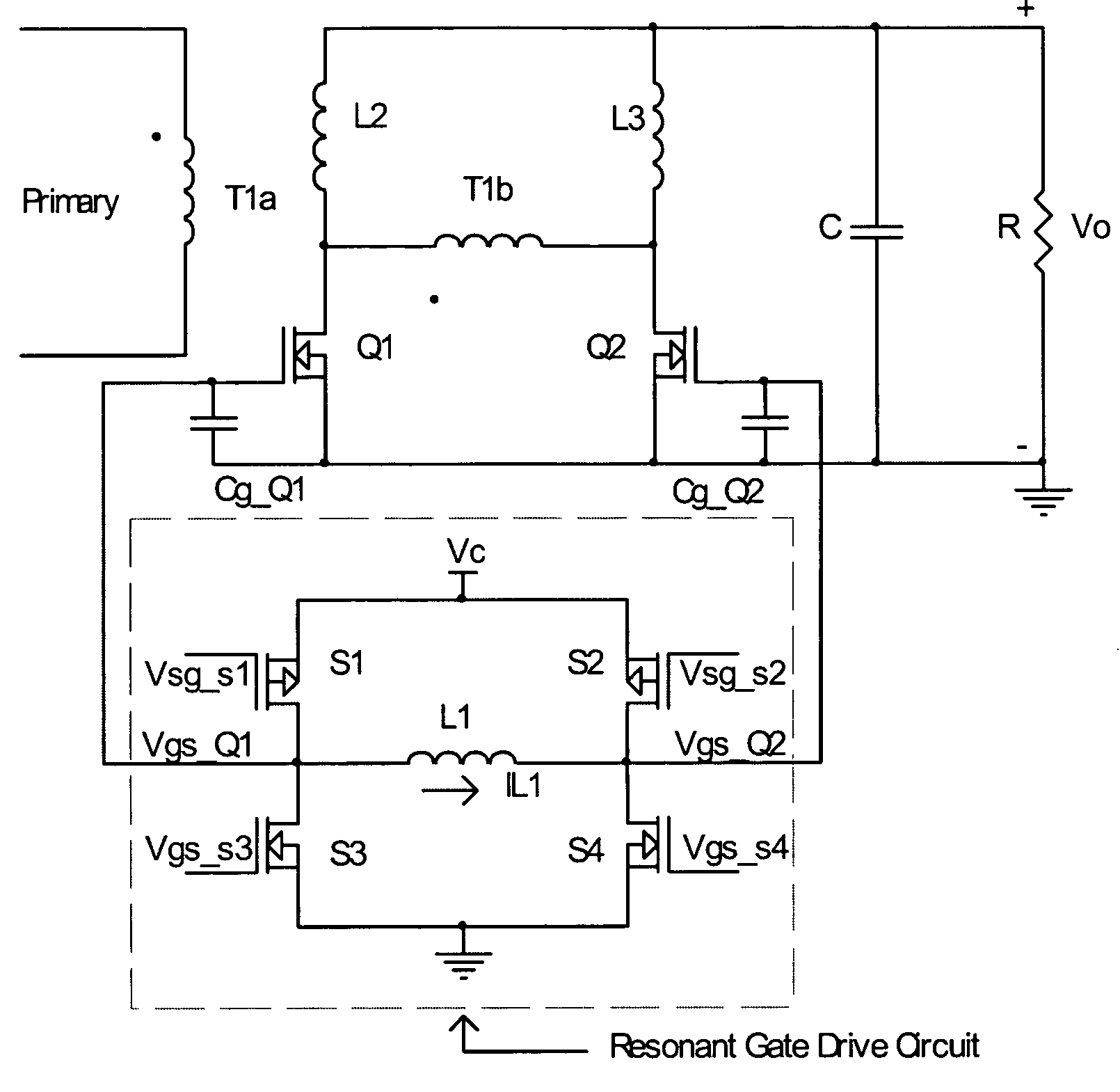
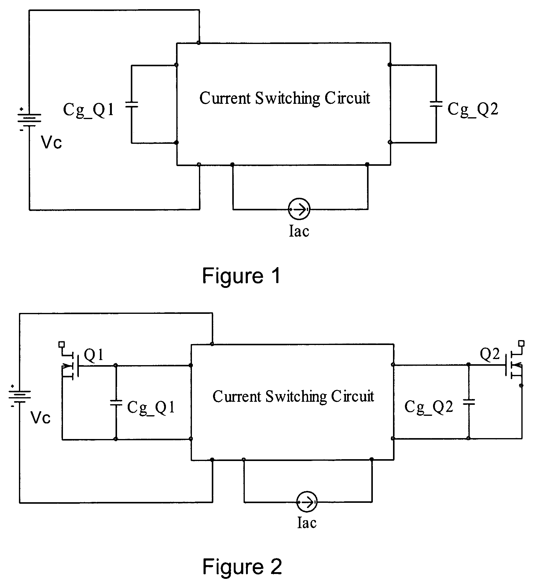
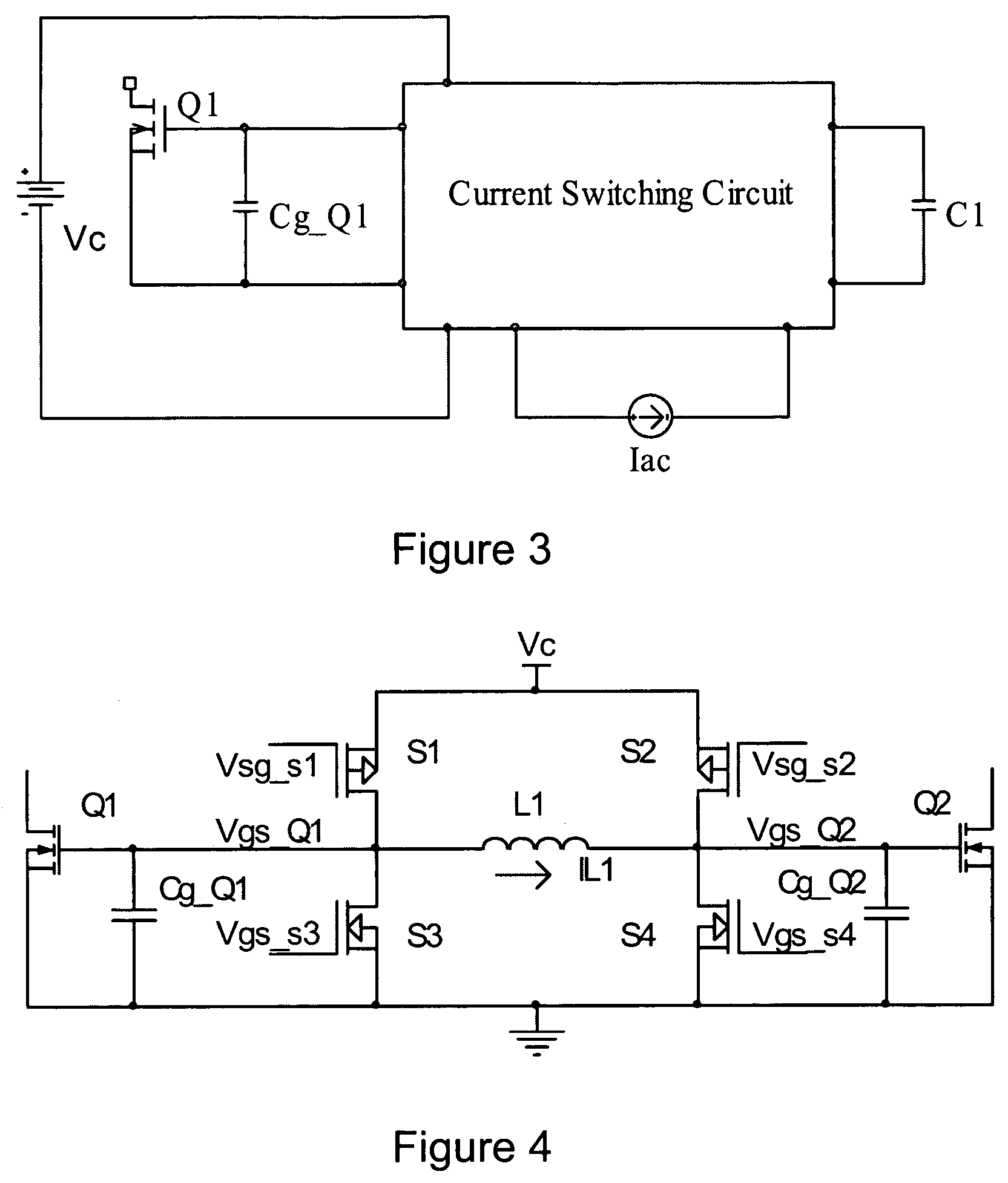
[0011]One object of the invention is to provide a resonant gate drive circuit to reduce the gate drive loss and other losses for power switching devices having an input capacitance.
[0012]Another object of the invention is to provide a resonant gate drive circuit that can drive two separate power switching devices with symmetrical signals to reduce the gate drive loss and conduction loss of the power switching devices.
[0013]Another object of the invention is to provide a resonant gate drive circuit that can drive two separate power switching devices with complementary signals to reduce the gate drive loss and conduction loss of the power switching devices.
[0014]Another object of the invention is to provide a resonant gate drive circuit that can drive low-side and high-side power switching devices with complementary or symmetrical signals to reduce gate drive loss, switching loss, and conduction loss of the power switching devices.SUMMARY OF THE INVENTION
[0019]wherein energy loss for charging and discharging the gate capacitance and switching loss of the said power switching device are reduced.

Problems solved by technology

Continued development of microprocessor and other integrated circuits introduces new challenges to the development of switching power converters.
As the operating frequency of power converters is raised, losses associated with driving the power MOSFET increase in proportion to the switching frequency.
At low power levels the resulting penalty on the overall converter efficiency become significant.
Therefore, in low voltage, high current applications, the gate drive loss will also increase when low on-resistance MOSFETs are chosen to reduce the conduction loss.
However, this approach makes the gate driver too complicated and limits the energy that can be recovered.
In general, the above solutions can only recover limited gate driving loss and provide little other benefit.
A resonant gate driver for two MOSFETs in a synchronous buck converter was proposed by K. Yao and F. C. Lee in “A novel resonant gate driver for high frequency synchronous buck converters,” IEEE Transactions on Power Electronics, 17:180-186 (2003), but the required control signals are difficult to generate, and the coupled inductor is expensive and difficult to design.
Further, that solution does not reduce the switching loss of the top MOSFET.
However, in that circuit, charging the gate capacitance with a low initial current resulted in the on-time of the power switch to be limited to a minimum of one-quarter of the resonant period of the L-C circuit, where C is the gate capacitance.
This placed a limit on the extent to which switching time and switching loss of the power switch could be reduced.
The derivative of the current (di / dt) is another important issue if the switching frequency is to be increased.

Method used


Image

  • Resonant gate drive circuits
  • Resonant gate drive circuits
  • Resonant gate drive circuits

Examples


embodiment 1 (

Reduced Pulse Embodiment 1 (2-Pulse)

[0171]If pulse 2 is eliminated from S2 and pulse 5 is eliminated from S4 in FIG. 22(a), energy can be saved for these switches in the form of gate loss and output loss (CV2) at turn-on. The body diodes (or external diodes) can be used to clamp the voltage across the inductor, allowing negligible current to circulate in the driver. In this case during the clamping interval t3-t4, switch S1 is on along with the body diode of S2. During the other clamping interval t7-t0, switch S3 is on along with the body diode of S4. Waveforms of this embodiment are shown in FIG. 22(b).

embodiment 2 (

Reduced Pulse Embodiment 2 (2-Pulse)

[0172]If pulse 3 is eliminated from S2 and pulse 6 is eliminated from S4 in FIG. 22(a), energy can be saved for these switches in the form of gate loss. The body diodes (or external diodes) can be used to provide the current paths when the energy is returned to the line. In this case during the energy return interval t2-t3, switch S1 is on along with the body diode of S4. During the other energy return interval t6-t7, switch S3 is on along with the body diode of S2. Waveforms of this embodiment are shown in FIG. 22(c)

embodiment 3 (

Reduced Pulse Embodiment 3 (1-Pulse)

[0173]The above two alternative embodiments may be combined by eliminating pulses 2 and 3 from S2, and pulses 5 and 6 from S4, in FIG. 22(a). Waveforms of this embodiment are shown in FIG. 22(d).

4.4 High-Side Drive Implementation

[0174]This resonant gate driver may be adapted for high-side drive of non-ground referenced MOSFET switches using a bootstrap circuit consisting of a diode, Db, and capacitor, Cb, as illustrated in FIG. 23. The equivalent gate capacitance of the power switch Q is not shown.

4.5 Dual High-Side and Low-Side Drive Implementation

[0175]The high-side driver shown in FIG. 23 may be utilized along with the low-side driver of FIG. 21 to drive both switches in a bridge-leg configuration, such as, for example, a synchronous buck converter, a full-bridge converter, a half-bridge converter, an active clamp forward converter, or a resonant converter with a full-bridge or half-bridge inverter. An example of such a circuit for driving a br...


PUM


Abstract

A resonate gate drive circuit for driving at least one power switching device recovers energy loss for charging and discharging the gate capacitance of the power switching devices. The gate drive circuit uses a current source to charge and discharge the gate capacitance with a high current, reducing the switching loss of the power switching device. The gate drive circuit comprises four semiconductor bidirectional conducting switching devices connected in a full-bridge configuration. An inductor connected across the bridge configuration provides the current source. The gate drive circuit may be used in single and dual high-side and low-side, symmetrical or complementary, power converter gate drive applications.

Description

RELATED APPLICATIONS[0001]This application is a continuation-in-part of U.S. patent application Ser. No. 11 / 045,055, filed Jan. 31, 2005, the contents of which are incorporated herein by reference in their entirety. This application also claims the benefit of U.S. Provisional Patent Application Ser. No. 60 / 733,213 filed Nov. 4, 2005, the contents of which are incorporated herein by reference in their entirety.FIELD OF THE INVENTION[0002]This invention relates to DC-DC and AC-DC switching converters. More particularly, it relates to an effective way to turn on and to turn off the power switch that is used in such converters.BACKGROUND OF THE INVENTION[0003]Continued development of microprocessor and other integrated circuits introduces new challenges to the development of switching power converters. In order to reduce the passive component size, and also to meet stringent transient response requirements, the switching frequency of power converters will move into the MHz range in the ...

Claims


Application Information

Patent Timeline
Patent Type & Authority Patents(United States)
IPC IPC(8): H03K17/74
CPCH02M1/08H02M1/088H02M3/3376H02M3/33592Y02B70/1475Y02B70/1433Y02B70/10
Inventor LIU, YAN-FEIYANG, ZHIHUAEBERLE, WILSON
Owner GANPOWER SEMICON FOSHAN LTD
Why Eureka
Try Eureka