Optical fiber array, optical component and optical switch using the optical fiber array

a technology of optical fiber array and optical fiber array, which is applied in the field of optical fiber array, can solve the problems of weak strength of exposed optical fiber, deformation of optical properties, and the inability to house or fix the entire optical fiber portion, and achieve the effects of reducing the number of components, low rigidity, and deformation

Inactive Publication Date: 2009-10-20
HITACHI METALS LTD
View PDF7 Cites 12 Cited by
  • Summary
  • Abstract
  • Description
  • Claims
  • Application Information

AI Technical Summary

Benefits of technology

[0015]The present invention has been made focusing attention on such problems, and is intended to provide optical fiber arrays having a structure to prevent the breaking or bending of coated optical fibers and also having a high positional accuracy, and the present invention is also intended to provide optical components and optical switches using the optical fiber array.
[0043]According to the present invention, it is possible to provide optical fiber arrays that prevent bending or breaking of coated optical fibers, the optical fiber arrays with high positional accuracy, and is also possible to provide optical components and optical switches using the optical fiber array.

Problems solved by technology

However, the optical fiber array using a substrate in which through-holes are formed has the following problems.
Although this optical fiber portion is inserted into a through-hole, the depth of the through-hole is shallow as compared with the length of the exposed optical fiber portion and thus the entire optical fiber portion may neither be housed nor be fixed.
The exposed optical fiber portion is weak in strength due to a lack of the protective coating, and sometimes is bent or broken in handling the opposite side of a tip to be inserted of the coated optical fiber.
Moreover, the bending causes a bending loss or bends the emitted light from the coated optical fiber to increase the interconnection loss when connecting with a filter element, and the like, thus causing a problem that the optical properties degrade.
Namely, in the case where a liquid phase etching or a gas phase etching in photolithography techniques is employed to form the through-hole, if the etched depth becomes deep, even if attempting to form a vertical through-hole, the inner-wall face of the hole is inclined from the direction perpendicular to the substrate face and becomes taper-shaped to increase the clearance between the coated optical fiber to be inserted, resulting in a problem of inclining the coated optical fiber.
Moreover, inconveniently, the etching time will increase and the manufacturing man-hour will increase.
Moreover, although the manufacture cost will be reduced if machining by a drill, or the like, is employed to form the through-hole, there is a problem in the positional accuracy since the bore diameter varies due to the wearing or misalignment of the drill, or the pitch between the holes varies due to a problem in the feeding accuracy of the stage.
However, this presents a problem that because the coating portion is bent by means of the angle alignment substrate, the position of the optical fiber of a coated optical fiber varies due to the elastic deformation or heat deformation of the coating, resulting in optical fibers that are inclined against the inner-wall face of the primary substrate.
The primary substrate and other substrate are offset from each other without sharing the axis line of a hole with respect to an coated optical fiber, and thus this does not arrange the coated optical fibers in a straight line to fix.
This method also has a problem that because this is a method for fixing the optical fiber using only one primary substrate, a optical fiber that is likely to be bent during assembly deviates from the hole and hits the primary substrate, so that the optical fiber is broken.

Method used


Image

  • Optical fiber array, optical component and optical switch using the optical fiber array
  • Optical fiber array, optical component and optical switch using the optical fiber array
  • Optical fiber array, optical component and optical switch using the optical fiber array

Examples


embodiment 1

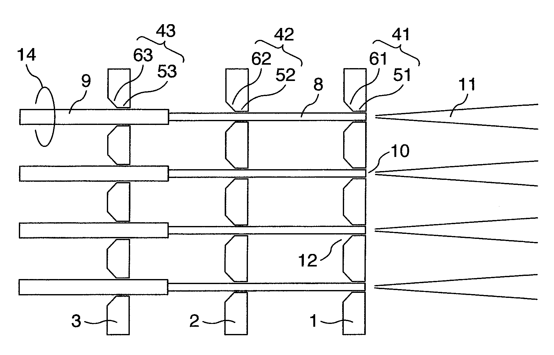
[0063]FIG. 1 is a cross sectional view showing an example of an optical fiber array concerning an embodiment of the present invention and FIG. 2 is the front view. In the optical fiber array shown in FIG. 1, a plurality of coated optical fibers 14; and a first substrate 1, second substrate 2, and third substrate 3 that have a plurality of through-holes 41, 42 and 43 for inserting the coated optical fibers; wherein the substrates have the through-holes opposingly arranged and are arranged in the order of the first substrate, the second substrate, and the third substrate. The each substrate serve as an alignment substrate for aligning the coated optical fibers 14. As shown in FIG. 1, the coated optical fiber 14 is inserted into the through-holes of the opposingly arranged first substrate, second substrate, and third substrate while a protective coating 9 at a tip thereof is removed so as to expose a optical fiber, wherein the through-holes 41 and 42 of the first and second substrates ...

embodiments 2 , 3

Embodiments 2, 3

[0092]For the reference of the pore shape, an optical fiber array in which the taper portion 61 of the first substrate is pyramid shaped and the bottom is a square of side length 140 μm (referred to as Reference Example 1), an optical fiber array in which the bottom is a square of side length 80 μm (referred to as Reference Example 2), and an optical fiber array in which the bottom is a square of side length 110 μm (referred to as Reference Example 3) were manufactured. The parallel pore 51 is in common, and the cross section is a circle with the diameters of 126 μm, which is the same as that of Embodiment 1. FIGS. 8A-8D are front views of the first substrate viewed from the fiber inserting side, i.e., viewed from the second substrate, FIG. 8A shows Embodiment 1, FIG. 8B shows Reference Example 1, FIG. 8C shows Embodiment 2, and FIG. 8D shows Embodiment 3.

[0093]In Reference Example 1, the diameter of the cross section of the parallel pore 51 is smaller than the diame...

embodiment 4

[0098]Moreover, in Embodiment 1, the optical fiber 8 and protective coating 9 of the coated optical fiber 14, and the through-holes 41, 42, and 43 are fixed by adhesive. Apart from this, an optical fiber array was prepared in the same way as Embodiment 1 except that the optical fiber 8 and the through-hole 41 are not fixed by adhesive (Embodiment 4). In Embodiment 4, the gap between the optical fiber 8 of the coated optical fiber 14 and the parallel pore 51 of the through-hole 41 is as extremely small as 1 μm and the optical fiber 8 is fitted therein, and thus the optical fiber 8 is fixed to the parallel pore 51 even without using adhesive. In this case, it is possible to prevent that the adhesive goes around to the coated optical fiber tip 10 to interfere with the emission of light, and further there is an advantage because the step of dripping adhesive may be saved. However, when the gap between the optical fiber 8 of the coated optical fiber 14 and the parallel pore 51 of the thr...


PUM


Abstract

An optical fiber array for insertion-positioning and arranging coated optical fibers in a substrate, in which a plurality of through-holes are formed, wherein a coating of a tip of the coated optical fiber is removed to expose a optical fiber, and wherein with the use of three substrates, the optical fiber of the coated optical fiber is inserted into through-holes of the first and second substrates and is positioned, and the coating of the coated optical fiber is inserted into a through-hole of the third substrate and is positioned.

Description

BACKGROUND OF THE INVENTION[0001]The present invention relates to optical fiber arrays, in which a plurality of coated optical fibers are arranged, the optical fiber arrays being widely used in optical components, optical system, and the like, and particularly relates to optical fiber arrays having the end face of the coated optical fibers arranged in two dimensions, and furthermore, the present invention relates to optical components, such as an optical switch, using the optical fiber array.[0002]In order to transmit and receive a large capacity of information at high speed, the optical fiber communications system has received attention. Today, coated optical fibers are installed not only between base stations in a big city, but even to terminals of each office building and each home, and dense optical fiber networks have been currently established. In relay points in the optical fiber network, a plurality of coated optical fibers are put together and the connection and switching o...

Claims


Application Information

Patent Timeline
Patent Type & Authority Patents(United States)
IPC IPC(8): G02B6/04G02B6/00
CPCG02B6/3582G02B6/3672G02B6/3512G02B6/3528G02B6/3548G02B6/3556G02B6/3644G02B6/3692
Inventor FURUSAWA, MITSUYASU
Owner HITACHI METALS LTD
Why Eureka
Try Eureka