Bridge resistance random access memory device with a singular contact structure

a memory device and resistance memory technology, applied in the direction of negative resistance effect devices, semiconductor devices, electrical appliances, etc., can solve the problems of large space occupation of contacts in resistance memory devices, and the manufacturing of such devices with very small dimensions, so as to reduce the overall dimension of memory cells

Active Publication Date: 2009-10-27
MACRONIX INT CO LTD
View PDF103 Cites 228 Cited by
  • Summary
  • Abstract
  • Description
  • Claims
  • Application Information

AI Technical Summary

Benefits of technology

[0012]Advantageously, the present invention reduces the overall dimension of a memory cell by having it share a single contact structure divided into two portions for use in connecting to a transistor and a bit line, eliminating the need for a second contact structure as required in a conventional design.

Problems solved by technology

Problems have arisen in manufacturing such devices with very small dimensions, and with variations in process that meet tight specifications needed for large-scale memory devices.
Contacts in a resistance memory device can occupy a significant amount of space.

Method used


Image

  • Bridge resistance random access memory device with a singular contact structure
  • Bridge resistance random access memory device with a singular contact structure
  • Bridge resistance random access memory device with a singular contact structure

Examples


first embodiment

[0034]FIG. 3 illustrates a cross-sectional view of a process diagram showing a first step in the manufacturing of a bistable resistive random access memory 300 with the formation of a transistor structure in accordance with the The bistable resistive random access memory 300 is formed on a semiconductor substrate 310. Access transistors are formed by an n-type terminal 312 acting as a common source region and n-type terminals 314 and 316 acting as drain regions in the p-type substrate 310. Polysilicon word (gate) lines 320, 322 form the gates of the access transistors. An inter-layer dielectric 330 includes dielectric fills 330a, 330b and 330c where the dielectric fill 330b is formed over the polysilicon word lines 320, 322. Suitable materials for implementing the inter-layer dielectric 330 include BPSG oxide and PETEOS oxide. The inter-layer dielectric 330 is patterned and conductive structures, including a common source line (not shown) and contact structures 326 and 328, are for...

third embodiment

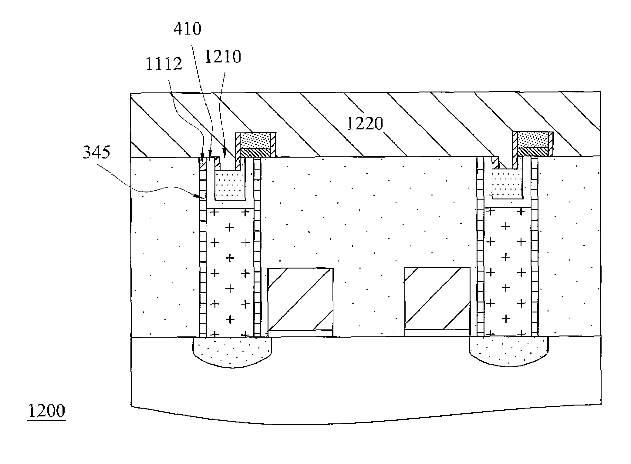
[0047]FIG. 10 is a process diagram 1000 illustrating a cross-sectional view of the bridge resistance random access memory with the deposition of a hard mask on a resistance memory material bridge. A top surface of the second electrode 420 is polished to remove excess materials that are outside the contact structures 326, 328, which results in a second electrode 420a in the first contact structure 326 and a second electrode 420b in the second contact structure 328. Embodiments of the process for polishing include a chemical mechanical polishing process, followed by brush clean and liquid and / or gas clean procedures, as known in the art. Alternatively, the chemical mechanical polishing may be conducted to an over-polish degree in order to enable the liner dielectric 410 that may protrude beyond the contact structure 326 to also be removed. The second electrode 420a is separated from the first electrode 345 by the thin liner dielectric 410. Top surfaces of the first electrode 345, the ...


PUM


Abstract

A resistance random access memory in a bridge structure is disclosed that comprises a contact structure where first and second electrodes are located within the contact structure. The first electrode has a circumferential extending shape, such as an annular shape, surrounding an inner wall of the contact structure. The second electrode is located within an interior of the circumferential extending shape and separated from the first electrode by an insulating material. A resistance memory bridge is in contact with an edge surface of the first and second electrodes. The first electrode in the contact structure is connected to a transistor and the second electrode in the contact structure is connected to a bit line. A bit line is connected to the second electrode by a self-aligning process.

Description

BACKGROUND OF THE INVENTION[0001]1. Field of the Invention[0002]The present invention relates to high density memory devices based on phase change based memory materials, including chalcogenide based materials and other materials, and to methods for manufacturing such devices.[0003]2. Description of Related Art[0004]Phase change based memory materials are widely used in read-write optical disks. These materials have at least two solid phases, including for example a generally amorphous solid phase and a generally crystalline solid phase. Laser pulses are used in read-write optical disks to switch between phases and to read the optical properties of the material after the phase change.[0005]Phase change based memory materials, like chalcogenide based materials and similar materials, also can be caused to change phase by application of electrical current at levels suitable for implementation in integrated circuits. The generally amorphous state is characterized by higher resistivity t...

Claims


Application Information

Patent Timeline
Patent Type & Authority Patents(United States)
IPC IPC(8): H01L29/04
CPCH01L45/04H01L45/16H01L27/2436H01L45/147H01L45/1226H01L45/144H01L45/146H01L45/06H10B63/30H10N70/231H10N70/20H10N70/823H10N70/8828H10N70/8833H10N70/8836H10N70/011
Inventor HO, CHIAHUALAI, ERH-KUNHSIEH, KUANG YEU
Owner MACRONIX INT CO LTD
Why Eureka
Try Eureka