

Liquid crystal display cell
a liquid crystal display and liquid crystal technology, applied in non-linear optics, instruments, optics, etc., can solve the problems of deterioration of contrast, inability to adequately reduce the transmittance in the black display condition, and inability to display moving pictures such as tv images, so as to reduce the internal reflection of at least the blue light component, prevent leakage, and facilitate the effect of retardation control
- Summary
- Abstract
- Description
- Claims
- Application Information
AI Technical Summary
Benefits of technology
Problems solved by technology
Method used
Image

Examples
embodiment 1
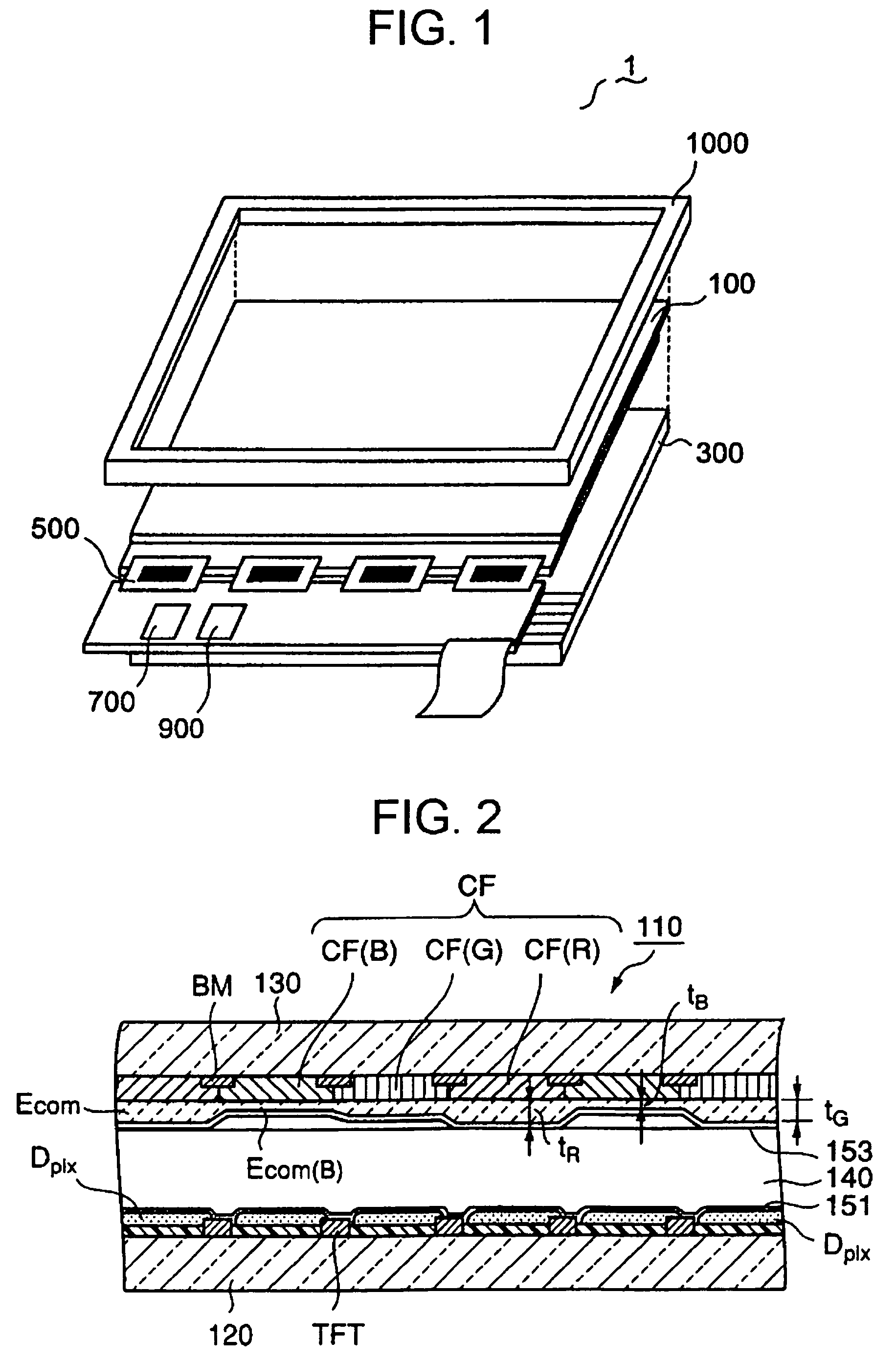
[0032]FIG. 1 shows a schematic block diagram of the liquid crystal display device according to the OCB mode system of the embodiment.
[0033]The liquid crystal display device 1 having the aspect ratio of 16:9 and the diagonal of 22 inches comprises a liquid crystal display panel 100 of light transmission active matrix type, a backlight 300 constituted of a plurality of tubular light sources 310 arranged in parallel together (Refer to FIG. 11) and located at the back of the liquid crystal display panel, scanning line drive circuits Ydr1, Ydr2 (Refer to FIG. 4) accommodated in the liquid crystal display panel 100 and supplying a scan signal Vg to a scanning line Yj, a signal line drive circuit 500 comprised of TCP (Tape Carrier Package) supplying a signal voltage Vsig to a signal line Xi (Refer to FIG. 4), an opposing electrode drive circuit 700 supplying an opposing electrode voltage Vcom to an opposing electrode Ecom (Refer to FIG. 2), and a control circuit 900 controlling the scannin...
embodiment 2
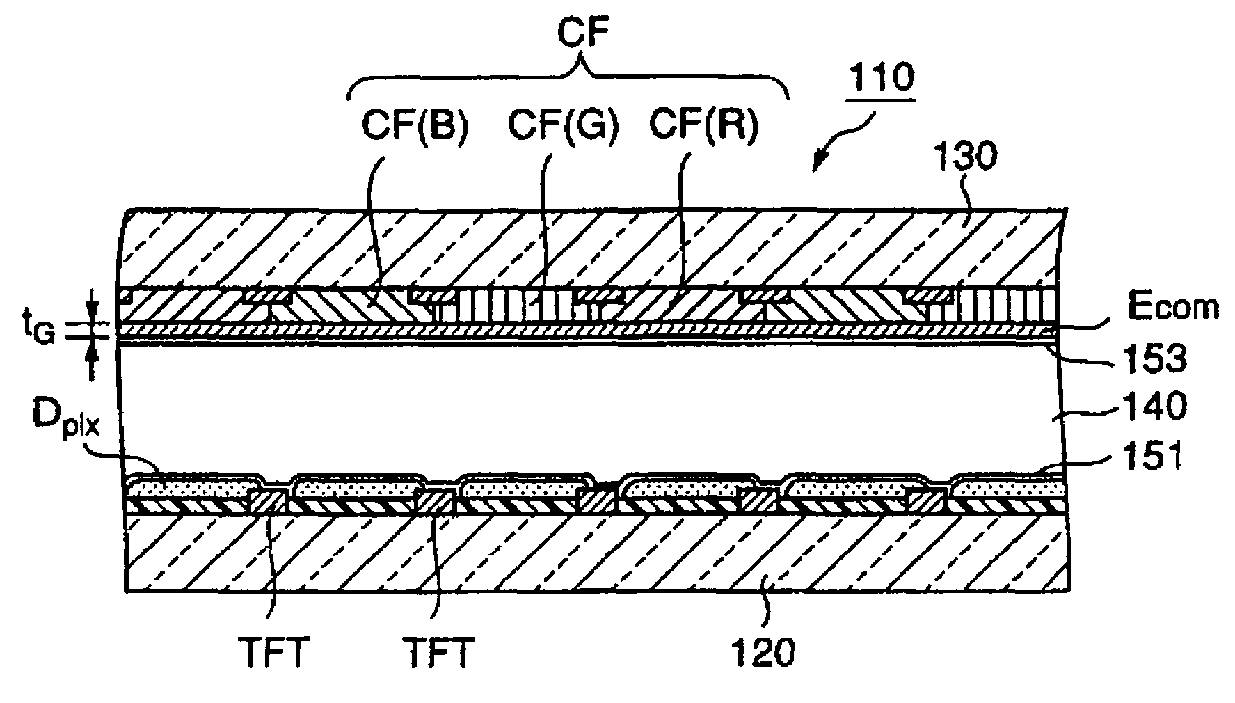
[0077]FIG. 12 shows the liquid crystal display cell 110 of the embodiment 2 of the present invention, having the same structure as FIG. 2 except that the structure of the opposing electrode Ecom is different from the structure explained by FIG. 2.
[0078]The opposing electrode Ecom of this embodiment has a uniform thickness regardless of each color filter layer, and the thickness is set to have the minimum value of the front reflectance at the range of blue region of 380 to 480 nm of the spectrum. Although it is needless to say that the optimum value should be designed at the place corresponding to the blue pixel in view of diminishing a tinge of blue, it is necessary that the thickness should not generate any deficiencies such as the contrast-deterioration also in the green pixel and the red pixel if the thickness of the opposing electrode is formed uniformly.
[0079]Specifically, the thickness in the case of indium tin oxide film of the refractive index 1.9 is set to be 116 nm when th...
embodiment 3
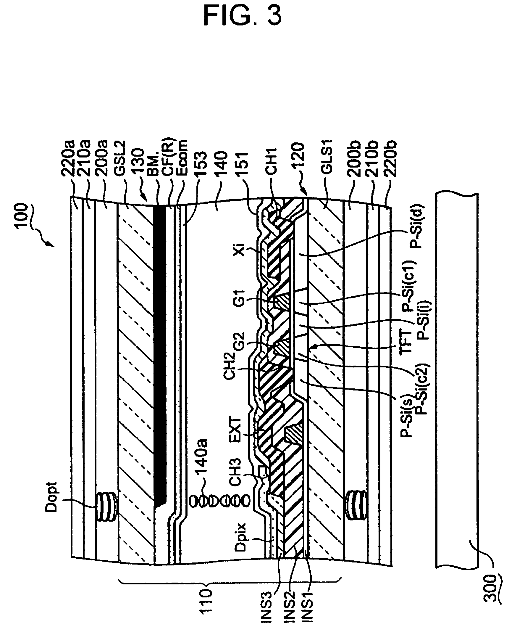
[0081]FIG. 13 shows an embodiment of the reflective type liquid crystal display device of OCB mode. Any portion denoted by the same mark as FIG. 9 shows the same portion, so that the explanation thereof will be omitted.
[0082]In addition, retardation is considered that the liquid crystal display cell is a reflective type. The birefringence anisotropy of liquid crystal material or the cell gap is adjusted so that the retardation is set to ½ of the above-mentioned embodiment.
[0083]For this reflective type liquid crystal display device 2, it is sufficient for the polarization plate that a sheet of the polarization plate 220a is placed at the front side. On the other hand, the reflection plate 160 is located at the rear side of the liquid crystal display cell 110. The natural light incident on the polarization plate 220a becomes a linearly polarized light with a component of the passing axis Ta of the polarization plate 220a. The light passes through the double axial phase difference pla...
PUM
| Property | Measurement | Unit |
|---|---|---|
| thickness | aaaaa | aaaaa |
| thickness | aaaaa | aaaaa |
| thickness | aaaaa | aaaaa |
Abstract
Description
Claims
Application Information