Inter-chip communication

a technology of inter-chip communication and microchips, applied in the direction of printed circuit aspects, sustainable manufacturing/processing, final product manufacturing, etc., can solve the problems of increasing power requirements and wasting considerable energy, and achieve the effect of reducing power dissipation, eliminating pin drivers and package capacitances

Active Publication Date: 2009-11-03
UNIV OF NOTRE DAME DU LAC
View PDF114 Cites 62 Cited by
  • Summary
  • Abstract
  • Description
  • Claims
  • Application Information

AI Technical Summary

Benefits of technology

[0007]It is one object of the present invention to provide an integrated system that provides reduced power dissipation through elimination of pin drivers and package capacitances.
[0008]It is one object of the present invention to provide a high performance integrated system that provides good signal integrity.
[0009]It is another object of the present invention to provide a high performance integrated system that provides high bandwidth.

Problems solved by technology

Also, a problem with current high-performance integrated systems is that they require increasing amounts of power and waste considerable energy in the form of heat.

Method used


Image

  • Inter-chip communication
  • Inter-chip communication
  • Inter-chip communication

Examples


example 1

[0212]3D electromagnetic simulations of interconnects on Si substrates using a simulated quilt packaging system of the present invention were conducted. The simulated quilt packaging systems provided: 1. Signal bandwidths>150 GHz 2. Low return loss / controllable impedance (˜20 dB return loss to 150 GHz predicted from simulations) 3. Very small excess delay (<75 fs) relative to on-chip interconnects. All of these performance metrics were achieved with simple, unoptimized structures.

example 2

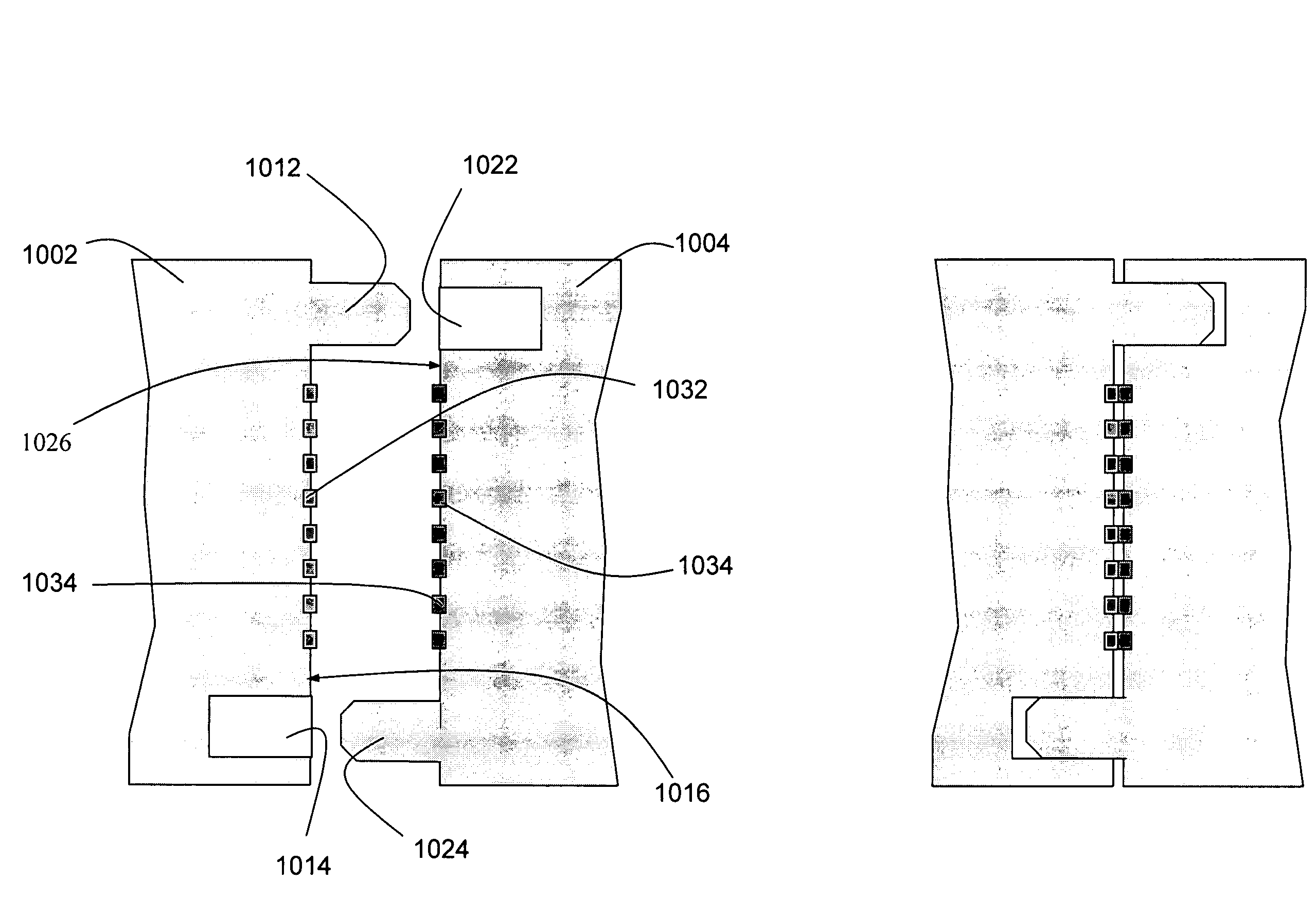
[0213]A procedure, similar to that described above with respect to FIGS. 2A-H was performed to form microchips of the present invention, with the exception that no additional metal interconnect layers were fabricated. A semiconductor wafer was formed in a conventional fashion to include die-on-wafer. Trenches were etched alongside edges of each microchip. Trenches for the edges of some microchips were shaped to produce male interconnect nodules and the trenches for the edges of other microchips were shaped to produce female interconnect nodules. Next, the exposed surfaces of the trenches were passivated by forming an oxide layer on the exposed surfaces of trenches by using a known semiconductor oxidation technique. Then a metal seed layer was evaporated on the whole wafer. Then a resist coating was applied. After the resist coating was applied, the resist coating was removed from everywhere but the trenches to protect the trenches. Then the metal seed layer was removed everywhere ex...


PUM


Abstract

The present invention provides a quilt packaging system for microchip, a method for making such a quilt packaging system, microchips that may be used in a such a quilt packaging system, and methods for making such microchips.

Description

CROSS-REFERENCE TO RELATED APPLICATIONS[0001]This application claims the priority now abandoned U.S. Provisional Patent Application. No. 60 / 499,885, entitled “Integration of Heterogeneous Communications Systems-in-Package,” filed Sep. 4, 2003 and the entire disclosure and contents of this provisional application is hereby incorporated by reference.BACKGROUND[0002]1. Field of the Invention[0003]The present invention relates generally to microchips and systems and devices employing microchips.[0004]2. Related Art[0005]There is currently a need in high-performance integrated systems for new approaches to device and circuit packaging that meet the extremely stringent performance demands of such systems in terms of signal integrity, bandwidth, and latency. Simultaneously, there is a need to meet such demands, while keeping the cost of such integrated systems low by making such systems easy to manufacture.[0006]Also, a problem with current high-performance integrated systems is that they ...

Claims


Application Information

Patent Timeline
Patent Type & Authority Patents(United States)
IPC IPC(8): H01L23/02H01L23/04H01L23/34
CPCH01L23/60H01L24/06H01L24/13H01L24/16H01L24/24H01L24/72H01L24/73H01L25/0652H01L25/0655H01L25/0657H01L25/16H01L25/18H01L29/0657H05K1/181H05K1/182H01L2223/6677H01L2224/05644H01L2224/05647H01L2224/13099H01L2224/18H01L2224/48227H01L2224/49175H01L2224/81224H01L2225/0651H01L2225/06551H01L2225/06562H01L2225/06596H01L2924/01014H01L2924/01015H01L2924/01029H01L2924/01046H01L2924/01078H01L2924/01079H01L2924/01082H01L2924/014H01L2924/10156H01L2924/10253H01L2924/10271H01L2924/10329H01L2924/14H01L2924/15311H01L2924/19041H01L2924/19042H01L2924/30105H01L2924/3011H01L2924/3025H01L2224/81141H01L24/48H01L24/49H05K3/326H05K3/328H01L2924/01005H01L2924/01006H01L2924/01019H01L2924/01023H01L2924/01033H05K2201/0314H05K2201/10454H05K2201/10909H01L2224/0401H01L2924/1461H01L2924/1305H01L2924/00014H01L2924/00H01L24/82Y02P70/50H01L2224/45099H01L2224/45015H01L2924/207H01L24/67H01L24/66H01L25/167
Inventor BERNSTEIN, GARY H.FAY, PATRICKPOROD, WOLFGANGLUI, QING
Owner UNIV OF NOTRE DAME DU LAC
Why Eureka
Try Eureka