Magnetic memory device and method of fabricating the same

a memory device and magnetic technology, applied in the field of magnetic memory devices, can solve the problems of not meeting all these requirements, still operating at low speeds, and sharply reducing the mr ratio of memory devices

Inactive Publication Date: 2009-11-03
SAMSUNG ELECTRONICS CO LTD
View PDF17 Cites 6 Cited by
  • Summary
  • Abstract
  • Description
  • Claims
  • Application Information

AI Technical Summary

Benefits of technology

[0015]Further, the exemplary embodiments of the present invention provide an MRAM, which has a high MR ratio without causing an increase in a switch field, and method of fabricating the same.
[0020]The MR enhancing layer may be formed to such a thickness so as to prevent AFC from occurring between the MR enhancing layer and the free layer. In an exemplary embodiment of the present invention, the MR enhancing layer may be formed to a thickness of about 3 to about 10 Å using one of an atomic layer deposition (ALD) technique and a chemical vapor deposition (CVD) technique.

Problems solved by technology

However, currently used memory devices, such as a static random access memory (SRAM), a dynamic random access memory (DRAM), and a flash memory, may not satisfy all these requirements.
Furthermore, the SRAM operates at high speed, but it is also a volatile memory device.
Further, although the flash memory is a nonvolatile memory device and (especially, for example, the NAND flash memory) has the highest integration density of present memory devices, it still operates at low speeds.
However, this high-temperature thermal treatment may lead to the intermixture of the free layer 40 and the capping layer 50, thereby sharply reducing the MR ratio.

Method used


Image

  • Magnetic memory device and method of fabricating the same
  • Magnetic memory device and method of fabricating the same
  • Magnetic memory device and method of fabricating the same

Examples


Embodiment Construction

[0028]Reference will now be made in detail to the exemplary embodiments of the present invention, examples of which are illustrated in the accompanying drawings. However, the present invention is not limited to the exemplary embodiments illustrated hereinafter.

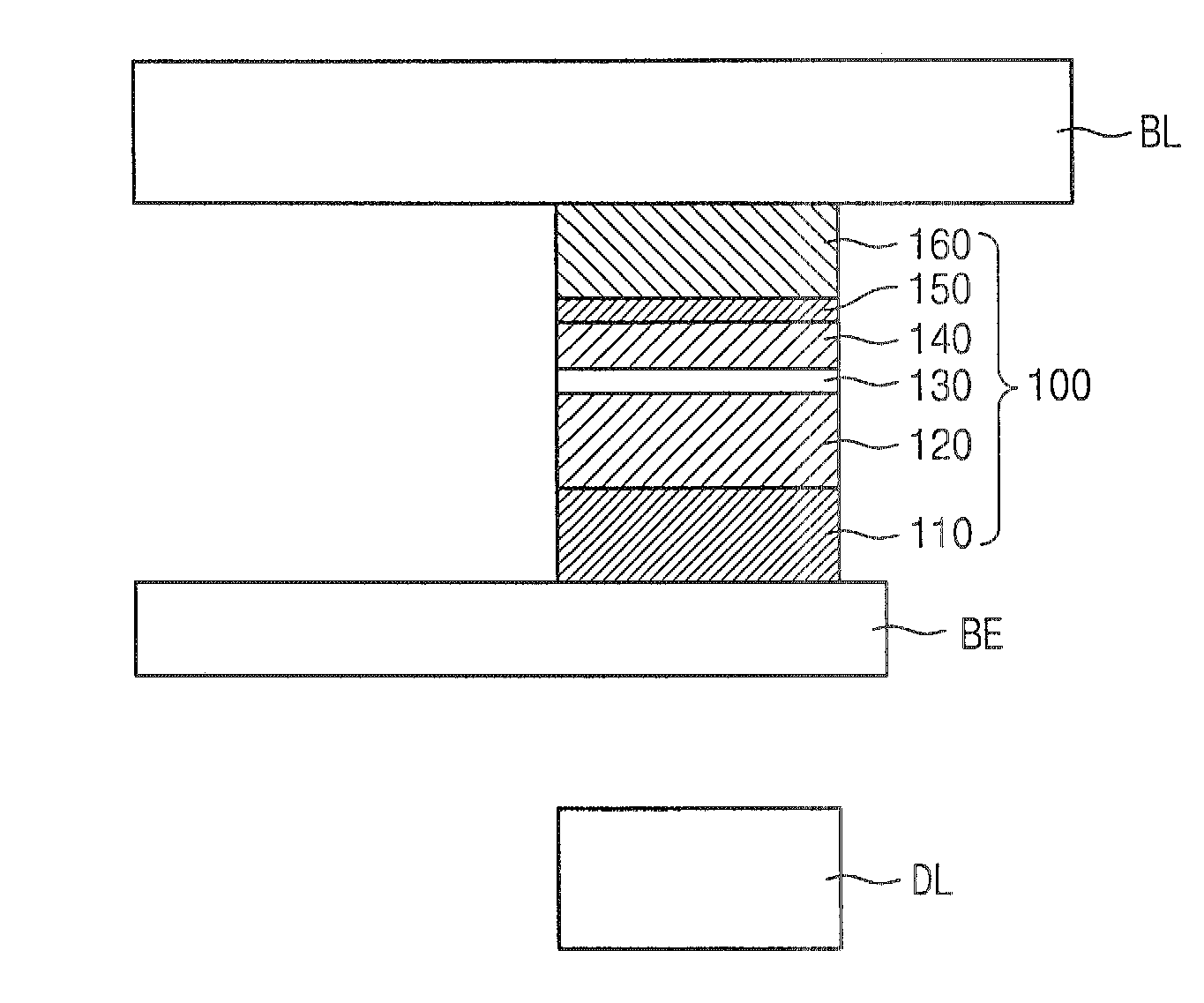
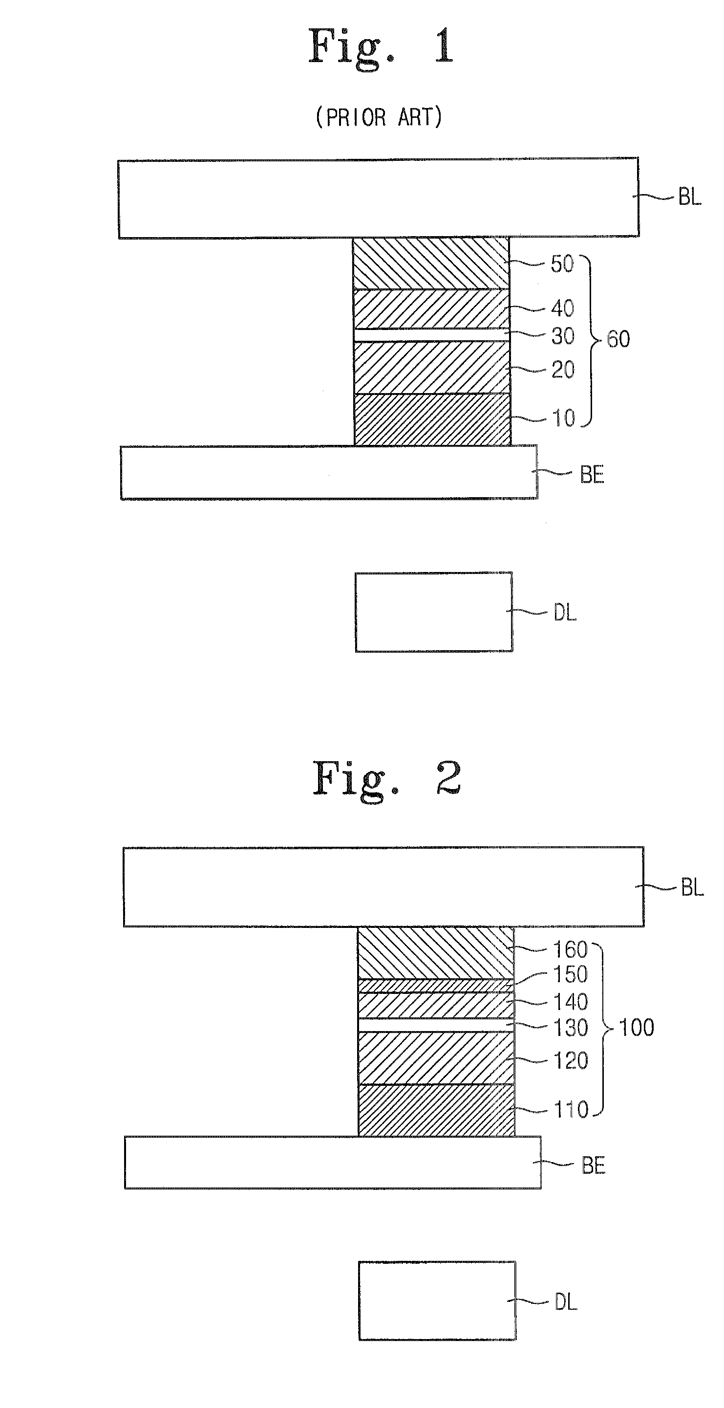
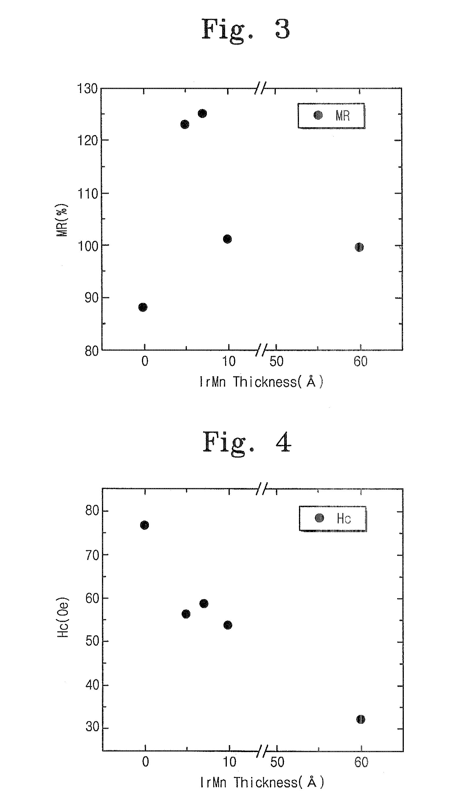
[0029]It will also be understood that when a layer is referred to as being “on” another layer or substrate, it can be directly on the other layer or substrate, or intervening layers may also be present. In the drawings, the thicknesses of layers and regions are exaggerated for clarity. It will be understood that although the terms first and second are used herein to describe various regions, layers and / or sections should not be limited by these terms. These terms are only used to distinguish one region, layer or section from another region, layer or section. Thus, for example, a first layer discussed below could be termed a first layer without departing from the teachings of the present invention. Each exemplary embodiment des...


PUM

PropertyMeasurementUnit
temperatureaaaaaaaaaa
thicknessaaaaaaaaaa
magnetoresistanceaaaaaaaaaa

Abstract

A magnetic memory device includes a pinning layer, a pinned layer, an insulation layer, which are sequentially stacked on a semiconductor substrate. The magnetic memory device further includes a free layer disposed on the insulation layer, a capping layer disposed on the free layer and an MR (magnetoresistance) enhancing layer interposed between the free layer and the capping layer. The MR enhancing layer is formed of at least one anti-ferromagnetic material.

Description

[0001]This application relies for priority upon Korean Patent Application No. 2006-08675, filed on Jan. 27, 2006, the contents of which are hereby incorporated by reference herein in their entirety.BACKGROUND OF THE INVENTION[0002]1. Technical Field[0003]The present disclosure relates to a semiconductor device and to a method of fabricating the same, and more particularly, to a magnetic memory device and to a method of fabricating the same.[0004]2. Description of the Related Art[0005]With the development of the electronics industry including, for example, mobile communications and computers, the demand for semiconductor devices having characteristics such as rapid read / write speed, nonvolatility, and a low operating voltage has increased. However, currently used memory devices, such as a static random access memory (SRAM), a dynamic random access memory (DRAM), and a flash memory, may not satisfy all these requirements.[0006]For example, as a unit cell of the DRAM typically includes...

Claims


Application Information

Patent Timeline
Patent Type & Authority Patents(United States)
IPC IPC(8): G11B5/39
CPCB82Y25/00B82Y40/00G01R33/093G11C11/16H01F10/3218H01F41/302H01L43/08H01L43/12H01F10/3254Y10T29/49044H01F10/3272H10N50/01H10N50/10
Inventor OH, SE-CHUNGLEE, JANG-EUNKIM, HYUN-JONAM, KYUNG-TAEJEONG, JUN-HO
Owner SAMSUNG ELECTRONICS CO LTD
Why Eureka
Try Eureka