Composite free layer within magnetic tunnel junction for MRAM applications

a technology of magnetic tunnel junction and free layer, applied in the direction of substrate/intermediate layer, magnetic body, instruments, etc., can solve the problems of poor writing margin, inability to directly apply structure in mram, degradation in one or more other parameters, etc., and achieve the effect of improving mram performan

Active Publication Date: 2015-10-13
TAIWAN SEMICON MFG CO LTD
View PDF18 Cites 4 Cited by
  • Summary
  • Abstract
  • Description
  • Claims
  • Application Information

AI Technical Summary

Benefits of technology

[0014]One objective of the present invention is to provide an improved MTJ element that enhances MRAM performance by decreasing the number of shorts and reducing the number of unswitched bits at a given bit line current compared with the prior art.
[0016]According to a first embodiment, these objectives are achieved with a MTJ element comprised of at least a pinned layer / tunnel barrier layer / free layer configuration wherein a composite free layer adjoins a surface of the tunnel barrier layer which is preferably MgO. A key feature is the composite free layer has a trilayer stack represented by FL1 / FL2 / FL3 where FL1 is a crystalline ferromagnetic layer adjoining the tunnel barrier layer and responsible for generating a high MR ratio in the MTJ. The FL2 layer is a second crystalline ferromagnetic layer that enables excellent switching performance without compromising the high MR ratio established by the tunnel barrier / FL1 configuration. The FL3 layer is an amorphous layer preferably having a NiFeX composition where X is one of Hf, Zr, Nb, Mg, or Ta which reduces MTJ shorting without adversely affecting other MTJ properties. For example, a CoFe / Fe / NiFeHf composite free layer is especially suited to realize the objectives and advantages of the present invention. Preferably, the CoFe layer has an Fe content of 60 to 90 atomic %, and the NiFeHf layer should be in the range of 20 to 40 Angstroms thick to provide the full advantage of a reduced number of shorted bits and a substantially lower bit switching current. The composite free layer may be formed in a bottom spin valve configuration represented by seed layer / AFM layer / pinned layer / tunnel barrier / FL1 / FL2 / FL3 / cap layer.

Problems solved by technology

Typically, an improvement in one property leads to a degradation in one or more other parameters.
In addition, recent developments show that a MgO / CoFeB tunnel barrier / free layer configuration exhibits very high MR ratio (>200%) but this structure could not be directly applied in MRAM because a MTJ with a CoFeB free layer shows very poor writing margin (wide bit-to-bit switching current) due to its high anisotropy energy.
Moreover, a high switch current is needed because of high coercivity associated with a CoFeB free layer.

Method used


Image

  • Composite free layer within magnetic tunnel junction for MRAM applications
  • Composite free layer within magnetic tunnel junction for MRAM applications
  • Composite free layer within magnetic tunnel junction for MRAM applications

Examples


first embodiment

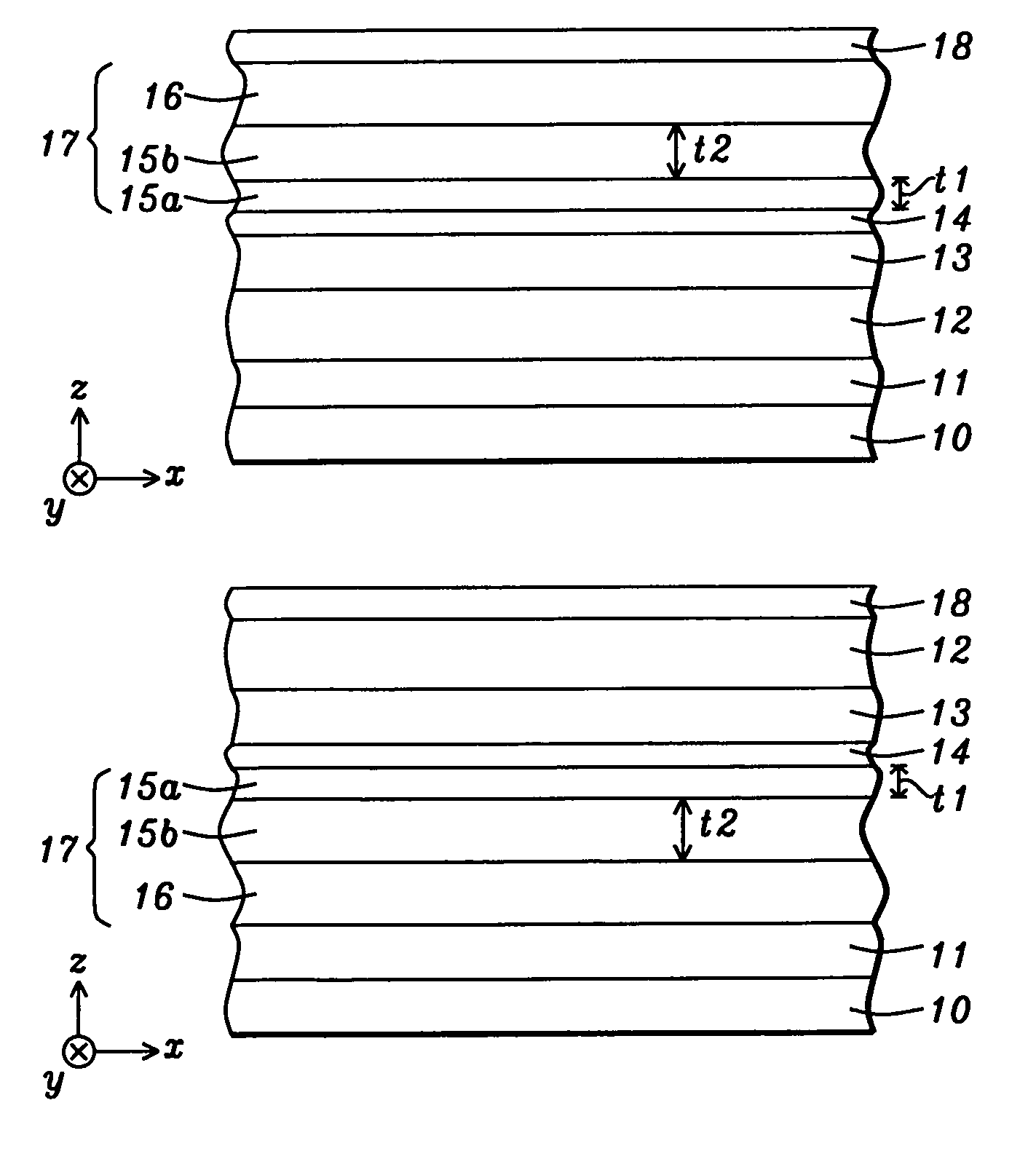
[0026]Referring to FIG. 1, a MTJ structure is illustrated according to the present invention. The substrate 10 may be a bottom conductor layer, for example, having a thickness in the z-axis direction and with a top surface in the x,y plane. A MTJ stack of layers is now formed on the substrate 10. It should be understood that all layers in the MTJ stack may be formed in the same process tool such as an Anelva C-7100 thin film sputtering system or the like which typically includes three physical vapor deposition (PVD) chambers each having 5 targets, an oxidation chamber, and a sputter etching chamber. At least one of the PVD chambers is capable of co-sputtering. Typically, the sputter deposition process involves an argon sputter gas and the targets are made of metal or alloys to be deposited on a substrate. All MTJ layers may be formed after a single pump down of the sputter system to enhance throughput.

[0027]In the exemplary embodiment depicting a bottom spin valve structure, the MTJ...

embodiment 1

[0044]In all examples except reference 4, a NiRFeSHfT layer where R=78, S=10, and T=12 was deposited by co-sputtering a Ni88Fe12 target and a Hf target in an Anelva 7100 sputter deposition system. The preferred deposition method comprises applying a forward power of 100 Watts (W) to 300 W to the Hf target and a forward power of 200 W to 600 W to the NiFe target to deposit a NiFeHf layer at a pressure less than about 0.3 mTorr and at an ambient temperature. As indicated in Table 1, the Embodiment 1 sample has a higher MR ratio and lower Hc and lower Hk than for the six reference samples which demonstrates that all three of the aforementioned properties can be optimized simultaneously by implementing a composite free layer according to the present invention. Note that a CoFeB free layer (Ref. 4) and a CoFe / NiFeHf composite free layer where a middle Fe layer has been omitted and CoFe thickness increased (Ref. 3) both afford significantly higher Hc and Hk that will degrade switching per...


PUM

PropertyMeasurementUnit
thicknessaaaaaaaaaa
thicknessaaaaaaaaaa
thicknessaaaaaaaaaa

Abstract

A magnetic tunneling junction (MTJ) in an MRAM array is disclosed with a composite free layer having a FL1 / FL2 / FL3 configuration where FL1 and FL2 are crystalline magnetic layers and FL3 is an amorphous NiFeX layer for improved bit switching performance. FL1 layer is CoFe which affords a high magnetoresistive (MR) ratio when forming an interface with a MgO tunnel barrier. FL2 is Fe to improve switching performance. NiFeX thickness where X is Hf is preferably between 20 to 40 Angstroms to substantially reduce bit line switching current and number of shorted bits. Annealing at 330° C. to 360° C. provides a high MR ratio of 190%. Furthermore, low Hc and Hk are simultaneously achieved with improved bit switching performance and fewer shorts without compromising other MTJ properties such as MR ratio. As a result of high MR ratio and lower bit-to-bit resistance variation, higher reading margin is realized.

Description

RELATED PATENT APPLICATIONS[0001]This application is related to the following: U.S. Pat. No. 7,528,457; U.S. Pat. No. 7,595,520; U.S. Pat. No. 7,663,131; U.S. Pat. No. 7,672,093; and Ser. No. 12 / 930,877; filing date Jan. 19, 2011; all assigned to a common assignee and herein incorporated by reference in their entirety.FIELD OF THE INVENTION[0002]The invention relates to a high performance Magnetic Tunneling Junction (MTJ) element and a method for making the same, and in particular, to a composite free layer comprised of a FL1 / FL2 / FL3 stack wherein FL1 is a first crystalline magnetic layer contacting a tunnel barrier layer, FL2 is a second crystalline magnetic layer, and FL3 is an amorphous layer to reduce MTJ shorting without adversely affecting the properties of the crystalline free layers.BACKGROUND OF THE INVENTION[0003]Magnetoresistive Random Access Memory (MRAM), based on the integration of silicon CMOS with MTJ technology, is a major emerging technology that is highly competit...

Claims


Application Information

Patent Timeline
Patent Type & Authority Patents(United States)
IPC IPC(8): H01L43/10H01L43/08H01F41/30B82Y40/00H01L43/12G11C11/16H01F10/187H01F10/32
CPCH01L43/10B82Y40/00G11C11/161H01F10/3295H01L43/08H01L43/12H01F41/303H01F10/3272H01F10/187H01F10/3254H10N50/85H10N50/10H10N50/01
Inventor CAO, WEIKULA, WITOLD
Owner TAIWAN SEMICON MFG CO LTD
Why Eureka
Try Eureka