
Methods of reducing coupling between floating gates in nonvolatile memory

a nonvolatile memory and floating gate technology, applied in the direction of basic electric elements, electrical equipment, semiconductor devices, etc., can solve the problems of limiting the amount of coupling in the overall layout, the difficulty of performing both of these functions, and the limit of how far a given circuit layout can be shrunk, so as to reduce the coupling

Inactive Publication Date: 2009-11-10
SANDISK TECH LLC
View PDF44 Cites 19 Cited by
  • Summary
  • Abstract
  • Description
  • Claims
  • Application Information

AI Technical Summary

Benefits of technology

The patent describes a process for making a nonvolatile memory array with floating gates that have an inverted-T shape. This shape reduces coupling between adjacent floating gates in the bit line direction, which improves performance. The process involves forming masking portions, using them to pattern the floating gate layer, and then removing them. The resulting structure has more space for a control gate and dielectric layer between adjacent floating gates in the word line direction. The process can be performed using various techniques and results in a memory array with improved performance.

Problems solved by technology

It is often difficult to perform both of these functions in an optimum manner with a single voltage.
But there are usually limits of how far a given circuit layout can be shrunk in this manner, since there is often at least one feature that is limited as to how much it can be shrunk, thus limiting the amount that the overall layout can be shrunk.

Method used


Image

  • Methods of reducing coupling between floating gates in nonvolatile memory
  • Methods of reducing coupling between floating gates in nonvolatile memory
  • Methods of reducing coupling between floating gates in nonvolatile memory

Examples


Embodiment Construction

Memory Operation

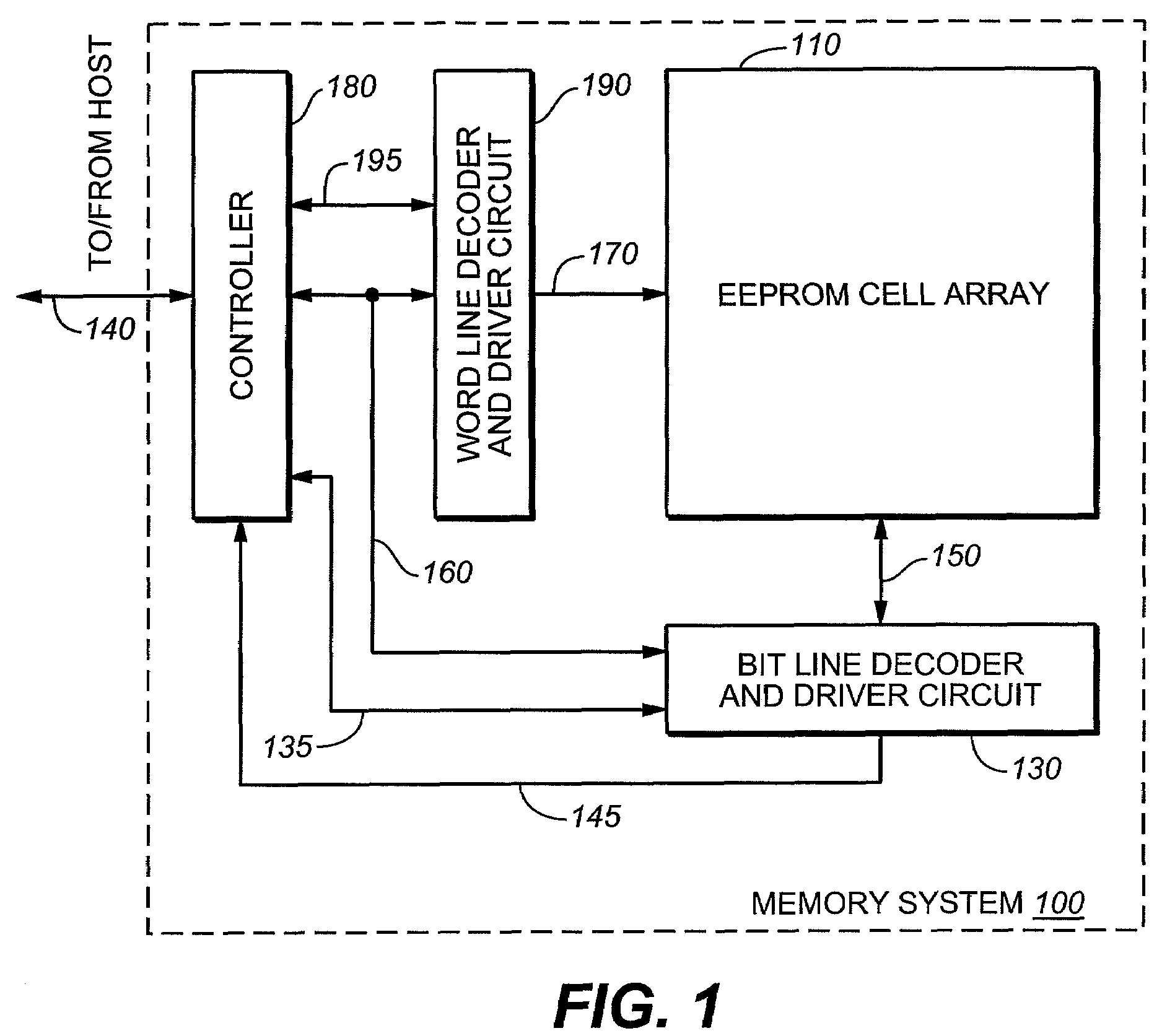
[0047]An example of a memory system 100 incorporating the various aspects of the present invention is generally illustrated in the block diagram of FIG. 1. A large number of individually addressable memory cells are arranged in a regular array 110 of rows and columns, although other physical arrangements of cells are certainly possible. Bit lines, designated herein to extend along columns of the array 110 of cells, are electrically connected with a bit line decoder and driver circuit 130 through lines 150. Word lines, which are designated in this description to extend along rows of the array 110 of cells, are electrically connected through lines 170 to a word line decoder and driver circuit 190. Each of the decoders 130 and 190 receives memory cell addresses over a bus 160 from a memory controller 180. The decoder and driving circuits are also connected to the controller 180 over respective control and status signal lines 135 and 195.

[0048]The controller 180 is conne...


PUM


Abstract

A nonvolatile memory array includes floating gates that have an inverted-T shape in cross section along a plane that is perpendicular to the direction along which floating cells are connected together to form a string. Adjacent strings are isolated by shallow trench isolation structures. An array having inverted-T shaped floating gates may be formed in a self-aligned manner.

Description

CROSS-REFERENCE TO RELATED APPLICATION[0001]This application is related to U.S. patent application Ser. No. 11 / 534,139, entitled, “Nonvolatile Memory with Reduced Coupling Between Floating Gates,” filed on the same day as the present application; which application is incorporated in its entirety by reference as if fully set forth herein.BACKGROUND OF THE INVENTION[0002]This invention relates generally to non-volatile flash memory systems, and, more specifically, to the structures of memory cells and arrays of memory cells, and to the process of forming them. All patents, patent applications and other documents cited in the present application are hereby incorporated by reference in their entirety.[0003]There are many commercially successful non-volatile memory products being used today, particularly in the form of small form factor cards, which use an array of flash EEPROM (Electrically Erasable and Programmable Read Only Memory) cells. In one type of architecture, a NAND array, a s...

Claims


Application Information

Patent Timeline
Patent Type & Authority Patents(United States)
IPC IPC(8): H01L21/336
CPCH01L21/28273H01L27/115H01L29/7881H01L29/42324H01L27/11521H01L29/40114H10B69/00H10B41/30
Inventor CHIEN, HENRYMATAMIS, GEORGEPHAM, TUANHIGASHITANI, MASAAKIHORIUCHI, HIDETAKALUTZE, JEFFREY W.MOKHLESI, NIMAFONG, YUPIN KAWING
Owner SANDISK TECH LLC
Learn More