Optical devices and related systems and methods

a technology of optical devices and optical elements, applied in the direction of optical radiation measurement, instruments, photomechanical equipment, etc., can solve the problems of incomplete individual optical elements contributing to the total intensity and phase non-uniformity of the system, and achieve the effect of enhancing the non-uniformity correction devi

Inactive Publication Date: 2009-12-08
CARL ZEISS SMT GMBH
View PDF19 Cites 5 Cited by
  • Summary
  • Abstract
  • Description
  • Claims
  • Application Information

AI Technical Summary

Benefits of technology

[0006]In some embodiments, the light beam intensity non-uniformity correction device includes an optical element having a light entrance face with a certain antireflective property. The antireflective property is locally amended in such a manner that the intensity uniformity of a light beam hitting the entrance face and e.g. transmitting the light beam intensity non-uniformity correction device is enhanced after having left the light beam intensity non-uniformity correction device.
[0007]The light entrance face of the light beam intensity non-uniformity correction device can have a uniform base antireflective property which is locally out of tune. While the antireflective property as such can prevent incoming light from being scattered and not being usable any more, the local maladjustment can eliminate locally undesired increased light intensities resulting in an improved homogenization of the light beam and therefore to an enhanced intensity uniformity.
[0008]In certain embodiments, the optical element is covered by an antireflective coating. The antireflective coating forms the entrance face. Any local amendment of the anti-reflective coating can result in an increased or decreased local reflectivity at the entrance surface. Locally amending the properties of the anti-reflective coating in a predetermined manner may serve for improving intensity uniformity of an incoming light beam.
[0019]Typically, the intensity distribution is measured in a field plane or a conjugate plane thereof. Measuring the intensity distribution in a field plane or a conjugate plane thereof, and in particular in the target plane has the advantage that it is quite easy to determine the locations where the corrections are to be done on the (at least) one of the optical elements.
[0023]A preferred method according includes the selecting of the one of the optical elements having the antireflective property being determined by an antireflective coating. Amending antireflective properties locally may easily achieved by means of locally using different materials or by adjusting the local thickness of the antireflective coating. The latter may be achieved by locally at least partly removing the antireflective coating or by locally depositing some more material.
[0052]Systems and methods disclosed herein can provide a light beam intensity non-uniformity correction device being capable of correcting intensity non-uniformities having variations up to 15% and the manufacturability of which is quite easy and therefore not expensive. The light beam in this case means not only visible light but also electromagnetic radiation from the far infrared to the very extreme ultraviolet spectral range, e.g. radiation frequencies between 0.15-11 μm, such as between 0.19-1.1 μm.

Problems solved by technology

In an optical system, consisting of a plurality of optical elements (as is the case for a laser annealing apparatus for carrying out such crystallization procedures), imperfections of the individual optical elements contribute to the total intensity and phase non-uniformity of the system.

Method used


Image

  • Optical devices and related systems and methods
  • Optical devices and related systems and methods
  • Optical devices and related systems and methods

Examples


Embodiment Construction

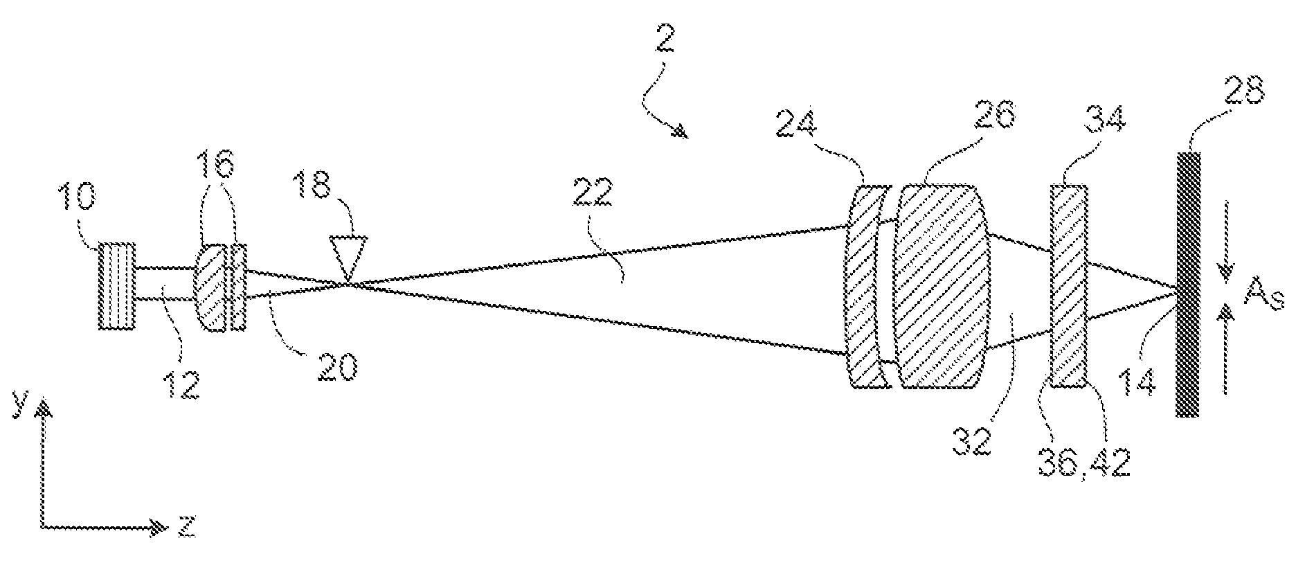
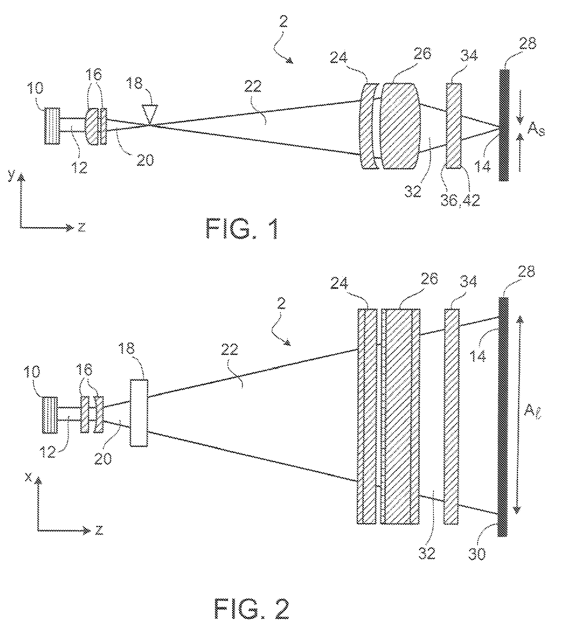
[0068]The description includes an anamorphic optical system which is capable for laser crystallization of an amorphous silicon layer.

[0069]Such an optical system is illustrated in FIGS. 1 and 2 and therein marked with the reference number 2. This optical system 2 comprises an excimer laser 10 which emits a pulsed beam 12 in per se known manner in z-direction. The dimensions of the excimer laser beam 12 emitted, for instance, may be 15 times 40 mm (in the xy-plane). The excimer laser 10 may preferably emit radiation in the spectral range between 130 nm and 390 nm. Instead of an excimer laser also a pulsed CO2-laser, a diode laser, a solid state laser or a frequency doubled solid state laser may be used.

[0070]This laser beam is imaged by means of the optical system 2 which will be specified below to yield an illuminating line 14 in a field plane 30.

[0071]The laser beam 12 emitted by the excimer laser 10 first passes an attenuator (not shown), if desired, and then enters a set of anamo...


PUM

PropertyMeasurementUnit
aspect ratioaaaaaaaaaa
diameteraaaaaaaaaa
depth of fieldaaaaaaaaaa

Abstract

The disclosure relates to a light beam intensity non-uniformity correction device that includes an optical element having a light entrance face with an antireflective property. According to the invention the antireflective property is locally amended in order to enhance light beam intensity uniformity. The disclosure further relates to a method for amending intensity distribution of a light beam in an optical system having one or more optical elements, where the method includes: a) assembling the optical system with the one or more optical elements arranged in predetermined positions, b) measuring intensity distribution, c) calculating locally required increase or decrease in absorption and / or reflection of one of the optical elements to amend measured intensity distribution into a predetermined intensity distribution, d) removing the optical element from the optical system, e) locally amending absorption and / or reflection of the one of the optical elements according to the calculation, f) installing the optical element in the predetermined position in the optical system.

Description

CROSS-REFERENCE TO RELATED APPLICATION[0001]This application claims the benefit under 35 U.S.C. §119(e)(1) of U.S. Provisional Application No. 60 / 731,313, filed Oct. 28, 2005, the contents of which are hereby incorporated by reference.FIELD[0002]The disclosure relates to a light beam intensity non-uniformity correction device that includes an optical element having a light entrance face with an antireflective property. The optical element can have at least one face covered with an anti-reflective coating. The disclosure further relates to a method for amending intensity distribution of a light beam in an optical system having one or more optical elements. The method can correct light beam intensity non-uniformity. The disclosure also relates to an anamorphic optical system for generating a sharp illuminating line on a surface, where the illuminating line can have a high aspect ratio and a cross-section with long and short axes. The disclosure relates to a scanning system for produci...

Claims


Application Information

Patent Timeline
Patent Type & Authority Patents(United States)
IPC IPC(8): G01J1/32G02B13/08
CPCG02B1/115G03F7/70975G02B27/0988G03F7/70591G03F7/70958G02B27/0966G02B5/22G02B13/08G02B1/11G02B27/00G03F7/20
Inventor SHKLOVER, VITALIYKIEREY, HOLGERMUENZ, HOLGERLE MAIRE, MICHELWEIGL, BERNHARD
Owner CARL ZEISS SMT GMBH
Why Eureka
Try Eureka