
Dipole induced transparency drop-filter cavity-waveguide system

a drop filter and transparent technology, applied in the direction of optical resonator shape and construction, instruments, optical elements, etc., can solve the problems of entanglement between the dipole and the reflected field, short cavity lifetime, and difficult to achieve using semiconductor technology

Inactive Publication Date: 2009-12-08
THE BOARD OF TRUSTEES OF THE LELAND STANFORD JUNIOR UNIV
View PDF5 Cites 4 Cited by
  • Summary
  • Abstract
  • Description
  • Claims
  • Application Information

AI Technical Summary

Benefits of technology

"This patent is related to the field of quantum information processing and semiconductor cavity quantum electrodynamics. The technical effects of this patent include the development of methods for implementing quantum repeaters using semiconductor systems and the removal of the necessity of using a strong coupling regime for dipoles and cavities, which can result in additional losses. The patent also discusses the use of cavity-dipole interactions to achieve complete switching in a more practical parameter regime for semiconductors and the need for quantum repeaters to overcome the limitations of optical communication due to large losses induced by optical channels. The patent includes various definitions and calculations related to the field of quantum information processing."

Problems solved by technology

This can result in entanglement between the dipole and reflected field.
Although this strong coupling regime has been attained in atomic systems, it is difficult to achieve using semiconductor technology.
Semiconductor implementations of cavity QED systems, such as photonic crystal cavities coupled to quantum dots, usually suffer from large out-of-plane losses, resulting in short cavity lifetimes. Things become even more difficult when one attempts to integrate cavities with waveguides.
At the same time, leakage into the waveguide introduces additional losses, making the strong coupling regime even more difficult to achieve.
One of the main limitations of quantum communication is that communication rates decay exponentially with distance due to large losses induced by optical channels.
This solution is not possible in quantum communication because amplification injects quantum noise into the channel, which destroys the state of the qubit.

Method used


Image

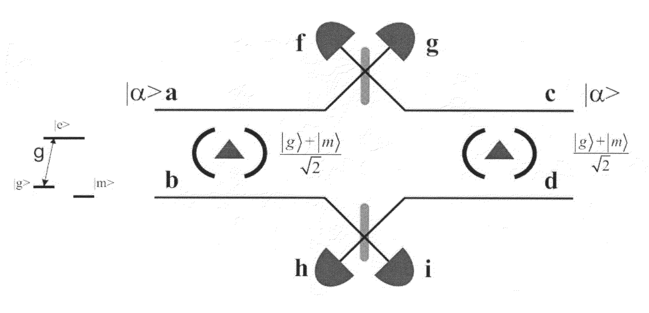
  • Dipole induced transparency drop-filter cavity-waveguide system
  • Dipole induced transparency drop-filter cavity-waveguide system
  • Dipole induced transparency drop-filter cavity-waveguide system

Examples


Embodiment Construction

[0026]Disclosed herein are systems and methods for switching a cavity between transmissive and reflective states in the weak coupling, bad cavity limit using the principle of dipole induced transparency (DIT). DIT also leads to entanglement between dipoles and fields which is a condition that can be exploited for quantum repeaters.

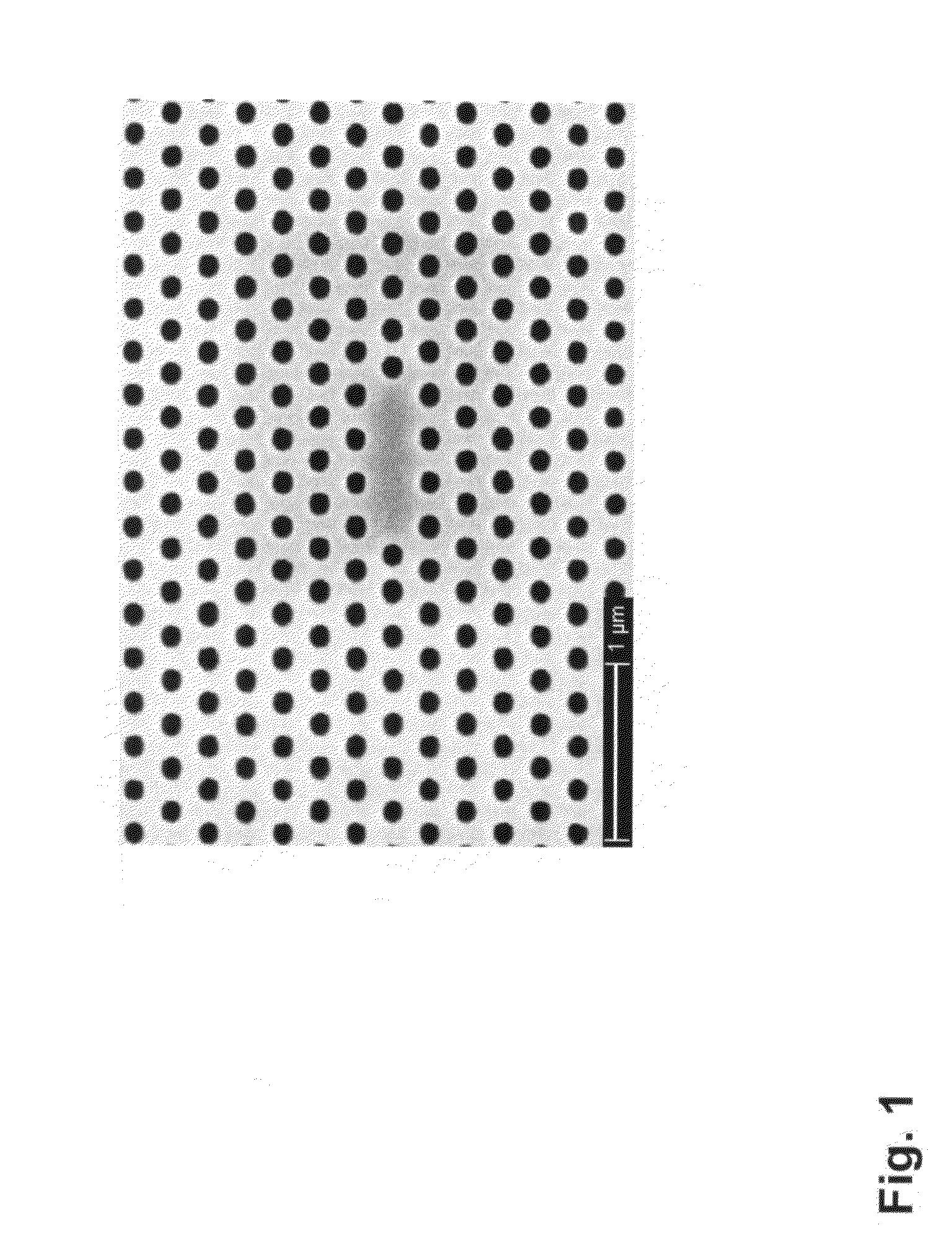
[0027]Some of the systems disclosed herein have been implemented, and experiments to validate basic principles have been performed, in planar photonic crystal (PC) devices in GaAs incorporating InAs quantum dots (QDs). A scanning electron micrograph of an optical cavity formed in a photonic crystal is shown in FIG. 1. The scale bar in the lower left corner of the figure is one micron long.

[0028]QD wafers are grown by molecular beam epitaxy. They generally contain an active region comprising a 150-160 nm thick GaAs layer with a centered InAs / GaAs QD layer. The active layer is grown on an AlGaAs sacrificial layer (with high Al content), which is in turn grow...


PUM

PropertyMeasurementUnit
thickaaaaaaaaaa
wavelengthsaaaaaaaaaa

Abstract

A normally opaque waveguide interacting with a drop-filter cavity can be switched to a transparent state when the drop filter is also coupled to a dipole. This dipole induced transparency may be obtained even when the vacuum Rabi frequency of the dipole is much less than the cavity decay rate. The condition for transparency is a large Purcell factor. Dipole induced transparency can be used in quantum repeaters for long distance quantum communication.

Description

RELATED APPLICATIONS[0001]This application claims priority benefit from U.S. provisional patent application No. 60 / 854,572 filed on Oct. 26, 2006 which is incorporated herein by reference.GOVERNMENT RIGHTS[0002]Inventions disclosed herein were made with U.S. Government support under contract DAAD19-03-1-0199 awarded by the U.S. Army Research Office. The Government has certain rights in the inventions.TECHNICAL FIELD[0003]The disclosure is generally related to semiconductor cavity quantum electrodynamics and quantum information processing.BACKGROUND[0004]Cavity quantum electrodynamics (CQED) offers promising approaches for implementing quantum information processing. Quantum networks combine the ease of storing and manipulating quantum information in atoms, ions, or quantum dots, with the advantages of transferring information between nodes via photons, using coherent interfaces. So far, demonstrations of basic building blocks of such networks have relied on atomic systems. Successfu...

Claims


Application Information

Patent Timeline
Patent Type & Authority Patents(United States)
IPC IPC(8): G02B6/26G02B6/42G02F1/035
CPCG02F1/365G02F2203/15G02F2202/32
Inventor WAKS, EDOVUCKOVIC, JELENA
Owner THE BOARD OF TRUSTEES OF THE LELAND STANFORD JUNIOR UNIV
Learn More