Method for forming AlGaN crystal layer

a technology of crystal layer and algan, which is applied in the direction of basic electric elements, electrical apparatus, semiconductor devices, etc., can solve the problems that crystal layer having a good surface flatness cannot be obtained, and the surface flatness of algan layer is not always good, so as to achieve good surface flatness

Inactive Publication Date: 2009-12-15
NGK INSULATORS LTD
View PDF1 Cites 3 Cited by
  • Summary
  • Abstract
  • Description
  • Claims
  • Application Information

AI Technical Summary

Benefits of technology

[0013]Accordingly, the second AlN layer is formed in a Ga-containing atmosphere so that it can be effective in relaxing the in-plane compressive stress applied on the first AlN layer as the surface layer of the template substrate, even though the second AlN layer has substantially the same composition as the first AlN layer.
[0015]It is therefore an object of the invention to provide a method for fabricating a high-Al-content AlGaN crystal layer with a good surface flatness.

Problems solved by technology

However, the inventors have found that when a high-Al-content AlGaN layer as disclosed in the article of Khan et al. is formed using a template substrate having the AlN surface layer, the resulting AlGaN layer does not always have a good surface flatness, although it has a good crystallinity.
In this case, however, crystal layers having a good surface flatness also cannot be obtained.

Method used


Image

  • Method for forming AlGaN crystal layer
  • Method for forming AlGaN crystal layer
  • Method for forming AlGaN crystal layer

Examples


examples

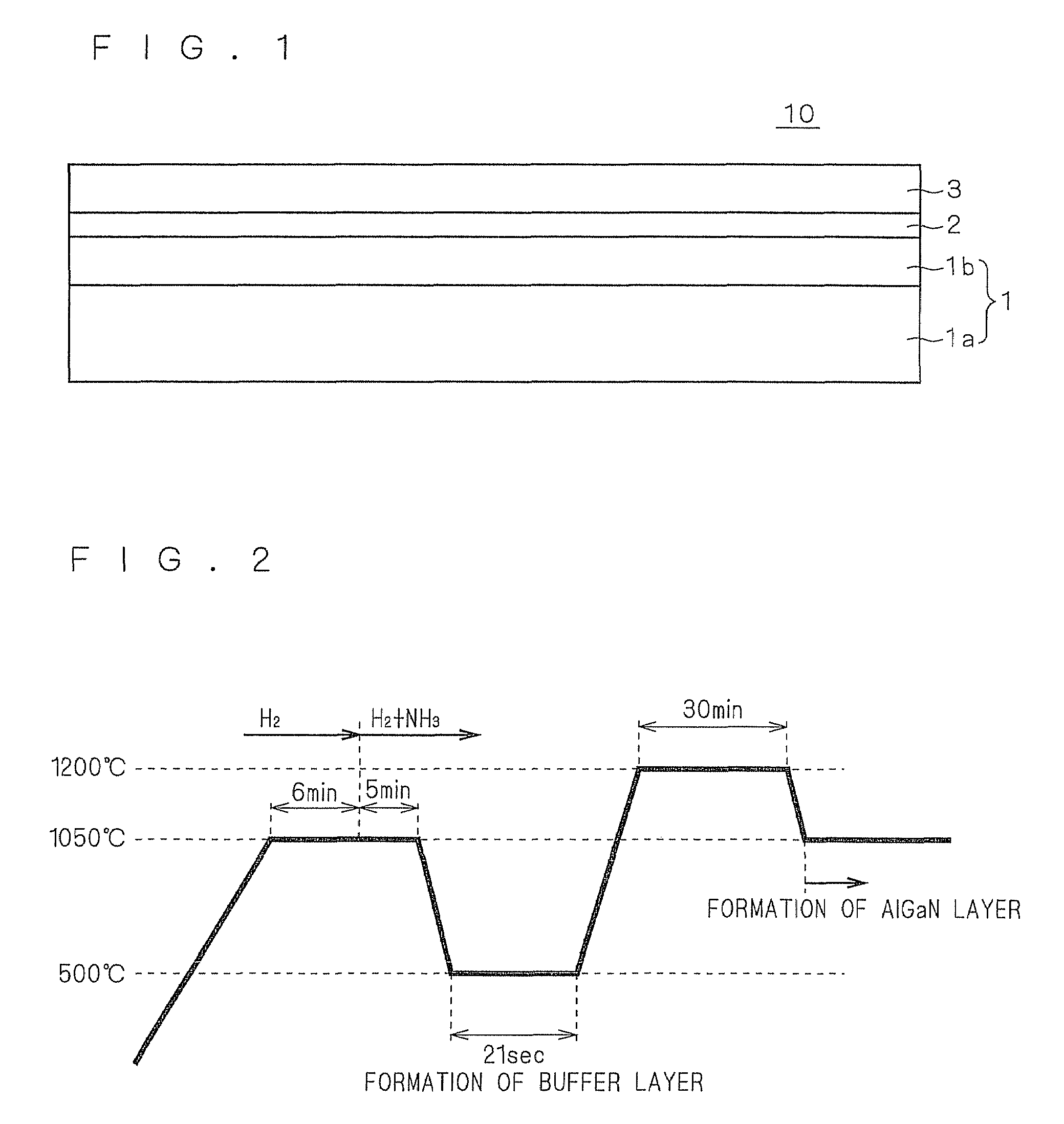
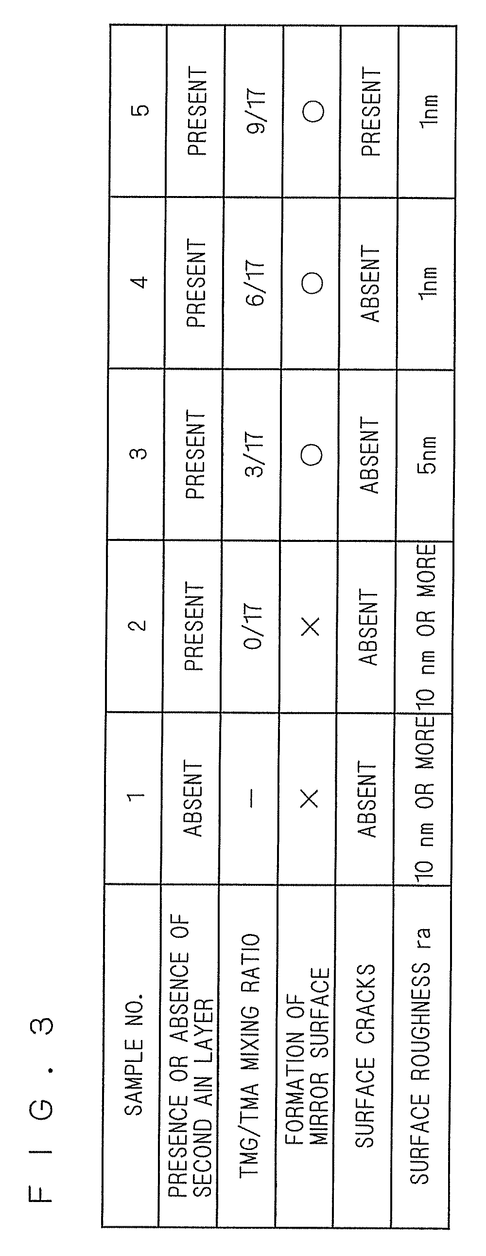
[0058]Buffer layers were formed under different forming conditions on template substrates prepared under the same conditions, respectively (including the case where no buffer layer was formed). AlGaN layers were formed under the same conditions on the different buffer layers, respectively, so that samples (Nos. 1 to 5) were prepared. The surfaces of the samples were each observed. In No. 1, the AlGaN layer was formed on the template substrate with no buffer layer. In Nos. 2 to 5, the feed rate of TMA was 17 μmol / minute, while the feed rate of TMG was 0, 3, 6, or 9 μmol / minute, in the process of forming the buffer layer.

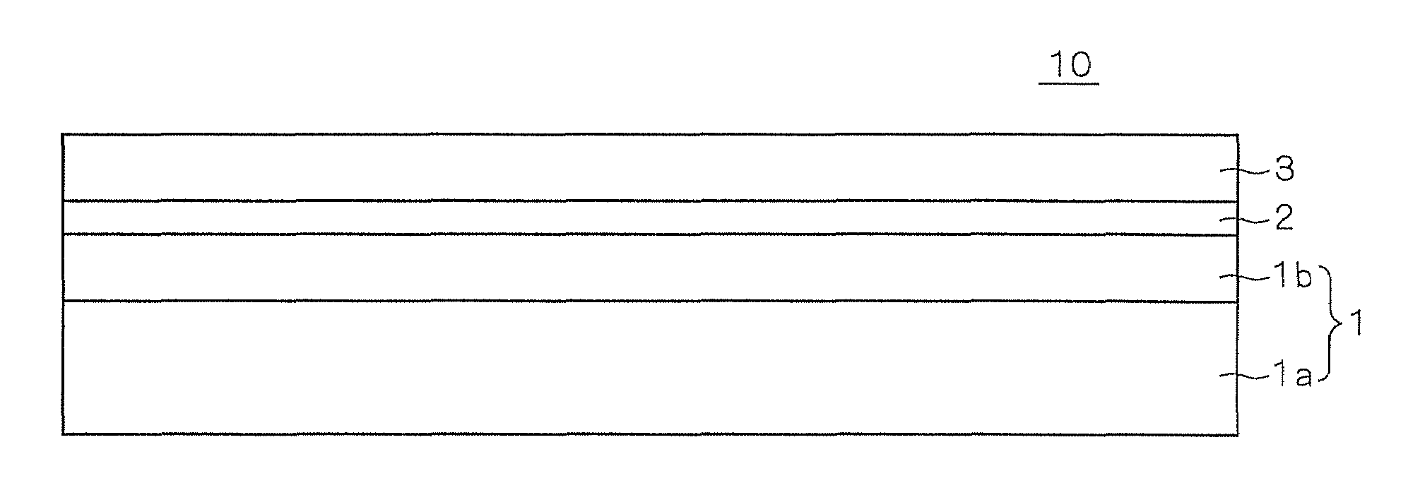
[0059]A 400 μm-thick, c-plane, sapphire single crystal was provided as a base material. A 1 μm-thick AlN layer was epitaxially grown on the base material using an MOCVD method and then heat-treated at 1700° C. in nitrogen, so that the template substrate was obtained. It was confirmed that in-plane compressive stress was applied to the surface layer (the first AlN laye...


PUM

PropertyMeasurementUnit
temperatureaaaaaaaaaa

Abstract

There is provided a method for preparing an AlGaN crystal layer having an excellent surface flatness. A buffer layer effective in stress relaxation is formed on a template substrate having a surface layer that is flat at a substantially atomic level and to which in-plane compressive stress is applied, and an AlGaN layer is formed on the buffer layer, so that an AlGaN layer can be formed that is flat at a substantially atomic level. Particularly when the surface layer of the template substrate includes a first AlN layer, a second AlN layer may be formed thereon at a temperature of 600° C. or lower, while a mixed gas of TMA and TMG is supplied in a TMG / TMA mixing ratio of 3 / 17 or more to 6 / 17 or less, so that a buffer layer effective in stress relaxation the can be formed in a preferred manner.

Description

BACKGROUND OF THE INVENTION[0001]1. Field of the Invention[0002]The invention relates to techniques for forming an AlGaN crystal layer on an AlN template substrate.[0003]2. Description of the Background Art[0004]There is a known technique for fabricating a template substrate (epitaxial substrate) that may be used as a base substrate in the process of epitaxially forming a Group III nitride crystal layer (see for example Japanese Patent Application Laid-Open (JP-A) No. 2006-332570).[0005]It is also known that a diode structure-type light-emitting device having an emission wavelength in the ultraviolet region is obtained by forming a light-emitting layer or an n-type or p-type conductive layer of high-Al-content AlxGa1−x N (x≧0.4) (see for example “III-Nitride UV Devices,” M. Asif Khan, M. Shatalov, H. P. Maruska, H. M. Wang, and E. Kuokstis, Jpn. J. Appl. Phys., Vol. 44, No. 10, 2005, pp. 7191-7206).[0006]In order to prepare a light-emitting device having an emission wavelength in th...

Claims


Application Information

Patent Timeline
Patent Type & Authority Patents(United States)
IPC IPC(8): H01L21/20H01L21/36H01L33/12H01L33/32
CPCH01L21/0237H01L21/0242H01L21/0262H01L21/02502H01L21/0254H01L21/02458
Inventor KOSAKA, KEISUMIYA, SHIGEAKISHIBATA, TOMOHIKO
Owner NGK INSULATORS LTD
Why Eureka
Try Eureka